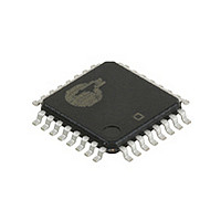
CY29947AC Cypress Semiconductor Corp, CY29947AC Datasheet - Page 2

CY29947AC
Manufacturer Part Number
CY29947AC
Description
Manufacturer
Cypress Semiconductor Corp
Type
Clock Driverr
Datasheet
1.CY29947AC.pdf
(7 pages)
Specifications of CY29947AC
Number Of Clock Inputs
2
Mode Of Operation
Single-Ended
Output Frequency
200MHz
Output Logic Level
LVCMOS/LVTTL
Operating Supply Voltage (min)
2.375V
Operating Supply Voltage (typ)
2.5/3.3V
Operating Supply Voltage (max)
3.63V
Package Type
TQFP
Operating Temp Range
0C to 70C
Operating Temperature Classification
Commercial
Signal Type
LVCMOS/LVTTL
Mounting
Surface Mount
Pin Count
32
Quiescent Current
7mA
Lead Free Status / RoHS Status
Not Compliant
Available stocks
Company
Part Number
Manufacturer
Quantity
Price
Company:
Part Number:
CY29947AC
Manufacturer:
CY
Quantity:
1 376
Pin Description
Note:
Output Enable/Disable
The CY29947 features a control input to enable or disable the
outputs. This data is latched on the falling edge of the input
clock. When SYNC_OE is asserted LOW, the outputs are dis-
abled in a LOW state. When SYNC_OE is set HIGH, the out-
puts are enabled as shown in Figure 1.
Document #: 38-07287 Rev. *C
1.
11, 13, 15, 19,
21, 23, 26, 28,
10, 14, 18, 22,
1, 8, 9, 12, 16,
17, 20, 24, 25,
PD = internal pull-down, PU = internal pull-up.
27, 31
29, 32
Pin
30
3
4
2
5
6
7
SYNC_OE
TCLK
Q
TCLK_SEL
SYNC_OE
[1]
TCLK0
TCLK1
Name
Q(8:0)
VDDC
VDD
VSS
TS#
VDDC
PWR
Figure 1. SYNC_OE Timing Diagram
I, PU
I, PU
I, PU
I, PU
I, PU
I/O
O
Test Clock Input
Test Clock Input
Test Clock Select Input. When LOW, TCLK0 is selected. When assert-
ed HIGH, TCLK1 is selected.
Clock Outputs
Output Enable Input. When asserted HIGH, the outputs are enabled
and when set LOW the outputs are disabled in a LOW state.
Three-state Control Input. When asserted LOW, the output buffers are
three-stated. When set HIGH, the output buffers are enabled.
3.3V or 2.5V Power Supply for Output Clock Buffers
3.3V or 2.5V Power Supply
Common Ground
Description
CY29947
Page 2 of 7
[+] Feedback


