DTC144TT1G ON Semiconductor, DTC144TT1G Datasheet

TRANS NPN BIAS RES 50V SC-59

DTC144TT1G

Manufacturer Part Number
DTC144TT1G
Description
TRANS NPN BIAS RES 50V SC-59
Manufacturer
ON Semiconductor
Datasheet

Specifications of DTC144TT1G

Transistor Type
NPN - Pre-Biased
Current - Collector (ic) (max)
100mA
Voltage - Collector Emitter Breakdown (max)
50V
Resistor - Base (r1) (ohms)
47K
Dc Current Gain (hfe) (min) @ Ic, Vce
160 @ 5mA, 10V
Vce Saturation (max) @ Ib, Ic
250mV @ 1mA, 10mA
Current - Collector Cutoff (max)
500nA
Power - Max
230mW
Mounting Type
Surface Mount
Package / Case
SC-59-3, SMT3, SOT-346, TO-236
Lead Free Status / RoHS Status
Lead free / RoHS Compliant
Other names
DTC144TT1GOS
DTC144TT1
Bias Resistor Transistor
NPN Silicon Surface Mount Transistor
with Monolithic Bias Resistor Network
device and its external resistor bias network. The BRT (Bias Resistor
Transistor) contains a single transistor with a monolithic bias network
consisting of two resistors; a series base resistor and a base−emitter
resistor. The BRT eliminates these individual components by
integrating them into a single device. The use of a BRT can reduce
both system cost and board space. The device is housed in the SC−59
package which is designed for low power surface mount applications.
Features
Maximum ratings are those values beyond which device damage can occur.
Maximum ratings applied to the device are individual stress limit values (not
normal operating conditions) and are not valid simultaneously. If these limits are
exceeded, device functional operation is not implied, damage may occur and
reliability may be affected.
1. FR−4 @ Minimum Pad
2. FR−4 @ 1.0 x 1.0 inch Pad
MAXIMUM RATINGS
© Semiconductor Components Industries, LLC, 2005
October, 2005 − Rev. 2
THERMAL CHARACTERISTICS
Collector-Base Voltage
Collector-Emitter Voltage
Collector Current
Total Device Dissipation
Derate above 25°C
Thermal Resistance,
Thermal Resistance,
Junction and Storage Temperature
This new series of digital transistors is designed to replace a single
ESD Rating
modified gull−winged leads absorb thermal stress during soldering
eliminating the possibility of damage to the die.
Simplifies Circuit Design
Reduces Board Space
Reduces Component Count
Moisture Sensitivity Level: 1
ESD Rating:
The SC−59 package can be soldered using wave or reflow. The
Pb−Free Package is Available
T
Junction-to-Ambient
Junction-to-Lead
Range
A
= 25°C
Characteristic
Rating
Human Body Model: Class 1
Machine Model: Class B
(T
A
= 25°C unless otherwise noted)
Preferred Devices
Symbol
Symbol
T
V
V
R
R
J
P
, T
CBO
CEO
I
qJA
qJL
C
D
stg
230 (Note 1)
338 (Note 2)
540 (Note 1)
370 (Note 2)
264 (Note 1)
287 (Note 2)
1.8 (Note 1)
2.7 (Note 2)
−55 to +150
Value
Max
100
50
50
1
mAdc
°C/W
°C/W
°C/W
Unit
Unit
Vdc
Vdc
mW
°C
See detailed ordering and shipping information in the package
dimensions section on page 2 of this data sheet.
Preferred devices are recommended choices for future use
and best overall value.
*Date Code orientation may vary depending
(INPUT)
upon manufacturing location.
(Note: Microdot may be in either location)
RESISTOR TRANSISTOR
BASE
PIN 2
ORDERING INFORMATION
NPN SILICON BIAS
8T
M
G
MARKING DIAGRAM
http://onsemi.com
= Specific Device Code
= Date Code*
= Pb−Free Package
R
R
1
CASE 318D
1
2
STYLE 1
1
SC−59
8T M G
Publication Order Number:
2
G
3
PIN 1
EMITTER
(GROUND)
PIN 3
COLLECTOR
(OUTPUT)
DTC144TT1/D

Related parts for DTC144TT1G

DTC144TT1G Summary of contents

Page 1

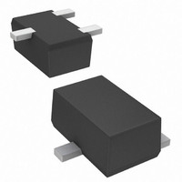
DTC144TT1 Preferred Devices Bias Resistor Transistor NPN Silicon Surface Mount Transistor with Monolithic Bias Resistor Network This new series of digital transistors is designed to replace a single device and its external resistor bias network. The BRT (Bias Resistor Transistor) ...

Page 2

... DEVICE MARKING AND RESISTOR VALUES Device DTC144TT1 DTC144TT1G †For information on tape and reel specifications, including part orientation and tape sizes, please refer to our Tape and Reel Packaging Specifications Brochure, BRD8011/D. ELECTRICAL CHARACTERISTICS Characteristic OFF CHARACTERISTICS Collector-Base Cutoff Current ( Collector-Emitter Cutoff Current ...

Page 3

TYPICAL APPLICATIONS FOR NPN BRTs +12 V FROM mP OR OTHER LOGIC Figure 2. Level Shifter: Connects Volt Circuits to Logic V CC OUT IN Figure 3. Open Collector Inverter: Inverts the Input Signal http://onsemi.com DTC144TT1 ISOLATED ...

Page 4

... A1 *For additional information on our Pb−Free strategy and soldering details, please download the ON Semiconductor Soldering and Mounting Techniques Reference Manual, SOLDERRM/D. ON Semiconductor and are registered trademarks of Semiconductor Components Industries, LLC (SCILLC). SCILLC reserves the right to make changes without further notice to any products herein. SCILLC makes no warranty, representation or guarantee regarding the suitability of its products for any particular purpose, nor does SCILLC assume any liability arising out of the application or use of any product or circuit, and specifically disclaims any and all liability, including without limitation special, consequential or incidental damages. “ ...

Related keywords