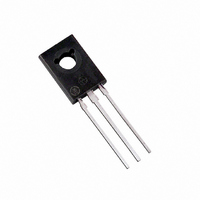
BD139 ON Semiconductor, BD139 Datasheet

TRANS NPN 1.5A 80V HPWR TO225AA

BD139

Manufacturer Part Number
BD139
Description
TRANS NPN 1.5A 80V HPWR TO225AA
Manufacturer
ON Semiconductor
Datasheet

Specifications of BD139

Transistor Type
NPN
Current - Collector (ic) (max)
1.5A
Voltage - Collector Emitter Breakdown (max)
80V
Vce Saturation (max) @ Ib, Ic
500mV @ 50mA, 500mA
Dc Current Gain (hfe) (min) @ Ic, Vce
40 @ 150mA, 2V
Power - Max
1.25W
Mounting Type
Through Hole
Package / Case
TO-225-3
Lead Free Status / RoHS Status
Contains lead / RoHS non-compliant
Current - Collector Cutoff (max)
-
Frequency - Transition
-
Other names
BD139OS

Available stocks

Company
Part Number
Manufacturer
Quantity
Price
Part Number:
BD139
Manufacturer:
FUJI
Quantity:
10 000
Part Number:
BD139
Manufacturer:
STM
Quantity:
100 000
Part Number:
BD139
Manufacturer:
ST
Quantity:
5 000
Part Number:
BD139
Manufacturer:
NXP
Quantity:
3 000
Part Number:
BD139
Manufacturer:
ST
0
Part Number:
BD139
Manufacturer:
ST
Quantity:
180
Part Number:
BD139
Manufacturer:
NXP/恩智浦
Quantity:
20 000
Part Number:
BD139
0
Company:
Part Number:
BD139
Quantity:
50 000
Company:
Part Number:
BD139
Quantity:
88 450
Company:
Part Number:
BD139
Quantity:
88 450
Part Number:
BD139-10
Manufacturer:
CDIL
Quantity:
20 000
Part Number:
BD139-10
Manufacturer:
ST
0
Part Number:
BD139-10
Manufacturer:
ST
Quantity:
20 000
Part Number:
BD139-10 (PB)
Manufacturer:
ST
0
Part Number:
BD139-16
Manufacturer:
ST
Quantity:
300
Part Number:
BD139-16
Manufacturer:
ON/安森美
Quantity:
20 000
Company:
Part Number:
BD139-16
Quantity:
9 000
Part Number:
BD139-ST
Manufacturer:
ST
0
BD135, BD137, BD139
Plastic Medium Power
Silicon NPN Transistor
designed for use as audio amplifiers and drivers utilizing
complementary or quasi complementary circuits.
Features
*For additional information on our Pb−Free strategy and soldering details, please
April, 2005 − Rev. 12
MAXIMUM RATINGS
Maximum ratings are those values beyond which device damage can oc-
cur. Maximum ratings applied to the device are individual stress limit values
(not normal operating conditions) and are not valid simultaneously. If these
limits are exceeded, device functional operation is not implied, damage
may occur and reliability may be affected.
THERMAL CHARACTERISTICS
download the ON Semiconductor Soldering and Mounting Techniques
Reference Manual, SOLDERRM/D.
Collector−Emitter Voltage
Collector−Base Voltage
Emitter−Base Voltage
Collector Current
Base Current
Total Device Dissipation @ T
Operating and Storage Junction
Temperature Range
Thermal Resistance,
Thermal Resistance,
This series of plastic, medium−power silicon NPN transistors are
Junction−to−Case
Junction−to−Ambient
Derate above 25 C
Derate above 25 C
Pb−Free Packages are Available
DC Current Gain − h
BD 135, 137, 139 are complementary with BD 136, 138, 140
Semiconductor Components Industries, LLC, 2005
Characteristic
Rating
FE
= 40 (Min) @ I
A
C
= 25 C
= 25 C
BD135
BD137
BD139
BD137
BD139
BD135
Symbol
Symbol
T
V
V
V
J
C
q
q
P
P
CEO
CBO
EBO
, T
I
I
JC
C
JA
B
D
D
= 0.15 Adc
stg
– 55 to
Value
+ 150
1.25
12.5
Max
100
100
100
5.0
1.5
0.5
45
60
80
45
60
10
10
mW/ C
mW/ C
Watts
Watts
Unit
Unit
Vdc
Vdc
Vdc
Adc
Adc
C/W
C/W
1
C
†For information on tape and reel specifications,
BD137G
BD135
BD135G
BD137
BD139
BD139G
including part orientation and tape sizes, please
refer to our Tape and Reel Packaging Specifications
Brochure, BRD8011/D.
1.5 A POWER TRANSISTORS
Device
3 2
ORDERING INFORMATION
45, 60, 80 V, 12.5 W
1
MARKING DIAGRAM
xx
Y
WW
http://onsemi.com
NPN SILICON
TO−225AA
TO−225AA
TO−225AA
TO−225AA
TO−225AA
TO−225AA
(Pb−Free)
(Pb−Free)
(Pb−Free)
Package
= 35, 37, 39
= Year
= Work Week
YWW
BD1xx
Publication Order Number:
TO−225AA
CASE 77
STYLE 1
500 Units/Box
500 Units/Box
500 Units/Box
500 Units/Box
500 Units/Box
500 Units/Box
Shipping
BD135/D

Related parts for BD139

BD139 Summary of contents

Page 1

... BD135, BD137, BD139 Plastic Medium Power Silicon NPN Transistor This series of plastic, medium−power silicon NPN transistors are designed for use as audio amplifiers and drivers utilizing complementary or quasi complementary circuits. Features Pb−Free Packages are Available DC Current Gain − (Min 135, 137, 139 are complementary with BD 136, 138, 140 ...

Page 2

... Adc 0.05 Adc Base−Emitter On Voltage 0.5 Adc 2.0 Vdc *Pulse Test: Pulse Width x 300 ms, Duty Cycle x 2.0%. 10.0 5.0 2.0 1.0 0.5 0.1 0.05 0.02 0.01 BD135, BD137, BD139 (T = 25_C unless otherwise noted) C Symbol CE(sat) V BE(on 0 125 BD135 BD137 ...

Page 3

... BD135, BD137, BD139 PACKAGE DIMENSIONS −B− −A− 0.25 (0.010 0.25 (0.010 TO−225AA CASE 77−09 ISSUE Z NOTES: 1. DIMENSIONING AND TOLERANCING PER ANSI Y14.5M, 1982. 2. CONTROLLING DIMENSION: INCH. 3. 077−01 THRU −08 OBSOLETE, NEW STANDARD 077−09. DIM MIN A 0.425 B 0.295 C 0 ...

Page 4

... P.O. Box 61312, Phoenix, Arizona 85082−1312 USA Phone: 480−829−7710 or 800−344−3860 Toll Free USA/Canada Fax: 480−829−7709 or 800−344−3867 Toll Free USA/Canada Email: orderlit@onsemi.com BD135, BD137, BD139 N. American Technical Support: 800−282−9855 Toll Free USA/Canada Japan: ON Semiconductor, Japan Customer Focus Center 2− ...

Related keywords