TIP142 ON Semiconductor, TIP142 Datasheet - Page 5
TIP142
Manufacturer Part Number
TIP142
Description
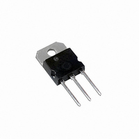
TRANS DARL NPN 10A 100V TO218AC
Manufacturer
ON Semiconductor
Datasheet
1.TIP147G.pdf
(7 pages)
Specifications of TIP142
Transistor Type
NPN - Darlington
Current - Collector (ic) (max)
10A
Voltage - Collector Emitter Breakdown (max)
100V
Vce Saturation (max) @ Ib, Ic
3V @ 40mA, 10A
Current - Collector Cutoff (max)
2mA
Dc Current Gain (hfe) (min) @ Ic, Vce
1000 @ 5A, 4V
Power - Max
125W
Mounting Type
Through Hole
Package / Case
SOT-93, TO-218 (Straight Leads)
Lead Free Status / RoHS Status
Contains lead / RoHS non-compliant
Frequency - Transition
-
Other names
TIP142OS
Available stocks
Company
Part Number
Manufacturer
Quantity
Price
Company:

Part Number:
TIP142
Manufacturer:
MUR
Quantity:
400 000
Company:
Part Number:
TIP142G
Manufacturer:
ON Semiconductor
Quantity:
500
Company:
Part Number:
TIP142G
Manufacturer:
ON
Quantity:
30 000
Part Number:
TIP142H
Manufacturer:
华奥DHA
Quantity:
20 000


NOTE 1: Input pulse width is increased until I
NOTE 2: For NPN test circuit reverse polarities.
a transistor: average junction temperature and second
breakdown. Safe operating area curves indicate I
limits of the transistor that must be observed for reliable
operation; i.e., the transistor must not be subjected to greater
dissipation than the curves indicate.
INPUT
There are two limitations on the power handling ability of
7.0
5.0
3.0
2.0
1.0
0.2
20
10
10
Figure 6. Active−Region Safe Operating Area
T
J
= 150°C
50
MPS−U52
V
SECONDARY BREAKDOWN LIMIT
BONDING WIRE LIMIT
THERMAL LIMITATION @ T
15
CE
, COLLECTOR−EMITTER VOLTAGE (VOLTS)
50
TIP140, TIP141, TIP142, (NPN); TIP145, TIP146, TIP147, (PNP)
20
R
= 100
TEST CIRCUIT
BB2
R
1.5 k
BB1
30
TIP140, 145
TIP141, 146
TIP142, 147
dc
V
BB1
C
V
BB2
ACTIVE−REGION SAFE OPERATING AREA
= 25°C
= 10 V
= 0
CM
50
= 1.42 A.
70
Figure 8. Inductive Load
V
TUT
CE
C
http://onsemi.com
MONITOR
− V
100 mH
R
V
S
CE
100
CC
= 0.1
= 20 V
MONITOR
5
I
C
variable depending on conditions. At high case
temperatures, thermal limitations will reduce the power that
can be handled to values less than the limitations imposed by
second breakdown.
The data of Figure 6 is based on T
7.0
5.0
2.0
1.0
15
10
VOLTAGE AND CURRENT WAVEFORMS
Figure 7. Unclamped Inductive Load
COLLECTOR
COLLECTOR
CURRENT
VOLTAGE
VOLTAGE
L, UNCLAMPED INDUCTIVE LOAD (mH)
0.5
V
V
(BR)CER
INPUT
1.42 A
CE(sat)
−20 V
1.0
2.0
100 ms
w ≈ 7.0 ms (SEE NOTE 1)
5.0
J(pk)
10
100 mJ
= 150_C; T
20
5.0 V
0
0
50
C
100
is
Related parts for TIP142
Image
Part Number
Description
Manufacturer
Datasheet
Request
R

Part Number:
Description:
ON Semiconductor [VOLTAGE REGULATOR]
Manufacturer:
ON Semiconductor
Datasheet:
Part Number:
Description:
357-036-542-201 CARDEDGE 36POS DL .156 BLK LOPRO
Manufacturer:
ON Semiconductor
Datasheet:
Part Number:
Description:
357-036-542-201 CARDEDGE 36POS DL .156 BLK LOPRO
Manufacturer:
ON Semiconductor
Datasheet:
Part Number:
Description:
357-036-542-201 CARDEDGE 36POS DL .156 BLK LOPRO
Manufacturer:
ON Semiconductor
Datasheet:
Part Number:
Description:
357-036-542-201 CARDEDGE 36POS DL .156 BLK LOPRO
Manufacturer:
ON Semiconductor
Datasheet:
Part Number:
Description:
357-036-542-201 CARDEDGE 36POS DL .156 BLK LOPRO
Manufacturer:
ON Semiconductor
Datasheet:
Part Number:
Description:
357-036-542-201 CARDEDGE 36POS DL .156 BLK LOPRO
Manufacturer:
ON Semiconductor
Datasheet:
Part Number:
Description:
357-036-542-201 CARDEDGE 36POS DL .156 BLK LOPRO
Manufacturer:
ON Semiconductor
Datasheet:
Part Number:
Description:
357-036-542-201 CARDEDGE 36POS DL .156 BLK LOPRO
Manufacturer:
ON Semiconductor
Datasheet:
Part Number:
Description:
357-036-542-201 CARDEDGE 36POS DL .156 BLK LOPRO
Manufacturer:
ON Semiconductor
Datasheet:
Part Number:
Description:
357-036-542-201 CARDEDGE 36POS DL .156 BLK LOPRO
Manufacturer:
ON Semiconductor
Datasheet:
Part Number:
Description:
Manufacturer:
ON Semiconductor
Datasheet:
Part Number:
Description:
Manufacturer:
ON Semiconductor
Datasheet:
Part Number:
Description:
Manufacturer:
ON Semiconductor
Datasheet: