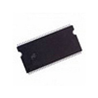
MT46V16M16P-5B IT:K Micron Technology Inc, MT46V16M16P-5B IT:K Datasheet - Page 56

MT46V16M16P-5B IT:K
Manufacturer Part Number
MT46V16M16P-5B IT:K
Description
DRAM Chip DDR SDRAM 256M-Bit 16Mx16 2.6V 66-Pin TSOP Tray
Manufacturer
Micron Technology Inc
Type
DDR SDRAMr
Datasheet
1.MT46V16M16P-5B_ITK.pdf
(93 pages)
Specifications of MT46V16M16P-5B IT:K
Density
256 Mb
Maximum Clock Rate
400 MHz
Package
66TSOP
Address Bus Width
15 Bit
Operating Supply Voltage
2.6 V
Maximum Random Access Time
0.7 ns
Operating Temperature
-40 to 85 °C
Organization
16Mx16
Address Bus
15b
Access Time (max)
700ps
Operating Supply Voltage (typ)
2.6V
Package Type
TSOP
Operating Temp Range
-40C to 85C
Operating Supply Voltage (max)
2.7V
Operating Supply Voltage (min)
2.5V
Supply Current
260mA
Pin Count
66
Mounting
Surface Mount
Operating Temperature Classification
Industrial
Lead Free Status / RoHS Status
Compliant
Figure 22:
PDF: 09005aef80768abb/Source: 09005aef82a95a3a
DDR_x4x8x16_Core2.fm - 256Mb DDR: Rev. O, Core DDR: Rev. B 1/09 EN
Command
BA0, BA1
Address
V
V
DQS
DD
V
CK#
CKE
A10
V
DM
DQ
CK
TT
REF
DD
Q
1
t VTD 1
INITIALIZATION Timing Diagram
Notes:
LVCMOS
LOW level
Power-up: V
T = 200µs
1. V
2. Although not required by the Micron device, JEDEC specifies issuing another LMR command
3. The two AUTO REFRESH commands at Td0 and Te0 may be applied following the LMR com-
4.
5. While programming the operating parameters, reset the DLL with A8 = 1.
(
(
(
(
(
(
(
)
(
)
)
)
)
)
(
(
(
(
(
(
)
(
(
(
(
(
)
)
)
)
)
)
)
)
)
)
)
)
(
(
(
(
(
(
(
(
(
(
)
(
(
)
(
)
(
)
(
)
(
)
(
(
(
)
)
)
)
)
)
)
)
)
)
)
)
)
V
even if V
the V
specified range.
(A8 = 0) prior to activating any bank. If another LMR command is issued, the same, previ-
ously issued operating parameters must be used.
mand at Ta0.
t
DESELECTs are allowed), and 200 cycles of CK are required before a READ command can be
issued.
MRD is required before any command can be applied (during MRD time only NOPs or
DD
TT
TT
t IS t IH
t IS
and CK stable
NOP
, and V
T0
is not applied directly to the device; however,
High-Z
High-Z
TT
t IH
t CH
t CK
supply and the input pin. Once initialized, V
DD
REF
/V
t CL
All banks
DD
t IS t IH
≤ V
PRE
T1
Q are 0V, provided a minimum of 42Ω of series resistance is used between
DD
+ 0.3V. Alternatively, V
t RP
(
(
(
(
(
(
(
(
(
(
)
(
)
(
)
(
)
(
)
(
)
(
)
)
)
)
)
)
)
)
)
)
(
(
(
(
(
(
(
(
(
(
)
(
)
(
)
(
)
(
)
(
)
(
)
)
)
Load extended
)
)
)
)
)
)
)
mode register
t IS t IH
t IS t IH
t IS t IH
BA0 = 1
BA1 = 0
Code
Code
LMR
Ta0
54
t MRD
(
(
(
(
(
(
(
(
(
)
)
(
)
(
)
(
)
(
)
(
)
(
)
(
)
)
)
)
)
)
)
)
(
(
(
(
(
(
(
(
(
)
)
(
)
(
)
(
)
(
)
(
)
(
)
(
)
)
)
)
)
)
)
)
Load mode
register5
Code 3
BA0 = 0
BA1 = 0
Code
LMR
Tb0
Micron Technology, Inc., reserves the right to change products or specifications without notice.
t MRD
(
(
(
(
(
(
(
TT
)
)
)
)
)
)
)
(
(
(
(
(
(
(
(
(
)
)
)
)
)
)
)
)
)
(
(
(
(
(
(
(
(
)
(
)
(
)
(
)
(
)
(
)
(
)
(
(
)
)
)
)
)
)
)
)
)
may be 1.35V maximum during power-up,
All banks
t IS t IH
PRE
256Mb: x4, x8, x16 DDR SDRAM
Tc0
t
VTD ≥ 0 to avoid device latch-up. V
REF
t RP
(
(
(
(
(
(
(
(
)
(
)
(
)
(
)
(
)
(
)
(
)
(
(
)
)
)
)
)
)
)
)
)
(
(
(
(
(
(
(
(
(
(
)
(
)
(
)
(
)
(
)
(
)
(
)
)
)
)
)
)
)
)
)
)
must always be powered within the
200 cycles of CK4
Td0
AR
Indicates A Break in
Time Scale
©2003 Micron Technology, Inc. All rights reserved.
t RFC
(
(
(
(
(
(
(
(
(
(
)
(
)
(
)
(
)
(
)
(
)
(
)
)
)
)
)
)
)
)
)
)
(
(
(
(
(
(
(
(
)
(
)
(
)
(
)
(
)
(
)
(
)
(
(
)
)
)
)
)
)
)
)
)
Te0
AR
t RFC
(
(
(
(
(
(
(
Operations
(
)
(
)
(
)
(
)
(
)
(
)
(
)
(
(
)
)
)
)
)
)
)
)
)
(
(
(
(
(
(
(
(
)
(
)
(
)
(
)
(
)
(
)
(
)
(
(
)
)
)
)
)
)
)
)
)
ACT 2
Don’t Care
Tf0
BA
RA
RA
DD
Q,


