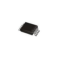
T5750-6AQJ71 Atmel, T5750-6AQJ71 Datasheet - Page 5

T5750-6AQJ71
Manufacturer Part Number
T5750-6AQJ71
Description
RF Transmitter UHF ASK/FSK Transmitter
Manufacturer
Atmel
Type
Transmitterr
Datasheet
1.T5750-6AQ.pdf
(13 pages)
Specifications of T5750-6AQJ71
Package / Case
TSSOP-8
Operating Frequency
868 MHz to 928 MHz
Maximum Operating Temperature
+ 125 C
Mounting Style
SMD/SMT
Operating Supply Voltage
2 V to 4 V
Supply Current
8.5 mA
Lead Free Status / RoHS Status
Lead free / RoHS Compliant
4.3
4.3.1
4.3.2
4546F–RKE–12/08
CLK Output
Clock Pulse Take-over
Output Matching and Power Setting
Figure 4-1.
Using C
tances on each side of the crystal of C
crystal of C
typical with worst case tolerances of ±16.8 kHz to ±28.0 kHz results.
An output CLK signal is provided for a connected microcontroller, the delivered signal is CMOS
compatible if the load capacitance is lower than 10 pF.
The clock of the crystal oscillator can be used for clocking the microcontroller. Atmel
ATARx9x has the special feature of starting with an integrated RC-oscillator to switch on the
T5750 with ENABLE = H, and after 4 ms to assume the clock signal of the transmission IC, so
that the message can be sent with crystal accuracy.
The output power is set by the load impedance of the antenna. The maximum output power is
achieved with a load impedance of Z
resistive path to V
The delivered current pulse of the power amplifier is 7.7 mA and the maximum output power is
delivered to a resistive load of 475 if the 0.53 pF output capacitance of the power amplifier is
compensated by the load impedance.
An optimum load impedance of:
Z
power of 5.5 dBm.
The load impedance is defined as the impedance seen from the T5750’s ANT1, ANT2 into the
matching network. Do not confuse this large signal load impedance with a small signal input
impedance delivered as input characteristic of RF amplifiers and measured from the application
into the IC instead of from the IC into the application for a power amplifier.
Less output power is achieved by lowering the real parallel part of 475 where the parallel imag-
inary part should be kept constant.
Output power measurement can be done with the circuit of
component values must be changed to compensate the individual board parasitics until the
T5750 has the right load impedance Z
the cable used to measure the output power must be calibrated out.
Load
= 475 || j/(2
4
= 9.2 pF ±2%, C
0
= 3.2 pF ±10% and a crystal with C
Tolerances of Frequency Modulation
XTAL
S
to deliver the DC current.
V
S
p
5
f
= 6.8 pF ±5%, a switch port with C
C
0.53 pF) = (166 + j226) thus results for the maximum output
Stray1
Load,opt
Load,opt
C
Stray1
M
= (166 + j226) at 868.3 MHz. There must be a low
L
= C
C
= (166 + j226) at 868.3 MHz. Also the damping of
M
0
Stray2
M
= 13 fF ±10%, an FSK deviation of ±21.5 kHz
R
S
= 1 pF ±10%, a parallel capacitance of the
Figure 4-2 on page
C
Switch
Stray2
C
5
= 3 pF ±10%, stray capaci-
C
Switch
C
4
6. Note that the
T5750
®
’s
5


