ST1510FX STMicroelectronics, ST1510FX Datasheet
ST1510FX
Specifications of ST1510FX
ST1510FX
Available stocks


Related parts for ST1510FX


ST1510FX Summary of contents
Page 1
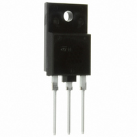
... The device is manufactured using Diffused Collector in Planar technology adopting new and enhanced high voltage structure 1 (E.H.V.S.1). Order codes Part number Marking ST1510FX 1510FX February 2007 High voltage fast-switching NPN Power transistor ISOWATT218FX Internal schematic diagram Package ISOWATT218FX Rev 2 ST1510FX Packing Tube 1/10 www.st.com 10 ...
Page 2
... Contents Contents 1 Electrical ratings . . . . . . . . . . . . . . . . . . . . . . . . . . . . . . . . . . . . . . . . . . . . 3 2 Electrical characteristics . . . . . . . . . . . . . . . . . . . . . . . . . . . . . . . . . . . . . 4 2.1 Electrical characteristics (curve 2.2 Test circuits . . . . . . . . . . . . . . . . . . . . . . . . . . . . . . . . . . . . . . . . . . . . . . . . . 7 3 Package mechanical data . . . . . . . . . . . . . . . . . . . . . . . . . . . . . . . . . . . . . 8 4 Revision history . . . . . . . . . . . . . . . . . . . . . . . . . . . . . . . . . . . . . . . . . . . 10 2/10 ST1510FX ...
Page 3
... ST1510FX Electrical ratings 1 Table 1. Absolute maximum rating Symbol V Collector-emitter voltage (V CES V Collector-emitter voltage (I CEO V Collector-base voltage (I EBO I Collector current C I Collector peak current ( Base current B P Total dissipation at T TOT Insulation withstand voltage (RMS) from all three leads to V isol external heatsink ...
Page 4
... Fall time f 1. Pulsed: Pulse duration = 300 ms, duty cycle 1.5% 4/10 Parameter Test conditions V = 1500V CE = 1500V 100mA -2.4A B(off 350V clamp ST1510FX Min. Typ. Max. 0.2 ° 125 750 1.5A 1 6.5 9 1.2A B(on 500µH 2 0.2 Unit mA mA ...
Page 5
... ST1510FX 2.1 Electrical characteristics (curve) Figure 1. Safe operating area Figure 3. Output characteristics Figure 5. DC current gain @ V Electrical characteristics Figure 2. Derating curve Figure 4. Reverse biased SOA =1V Figure 6. DC current gain @ V CE =5V CE 5/10 ...
Page 6
... Electrical characteristics Figure 7. Collector emitter saturation voltage 2.2 Test circuits Figure 9. Power losses and inductive load switching Figure 10. Reverse biased safe operating area 6/10 Figure 8. Base emitter saturation voltage ST1510FX ...
Page 7
... ST1510FX 3 Package mechanical data In order to meet environmental requirements, ST offers these devices in ECOPACK® packages. These packages have a Lead-free second level interconnect. The category of second level interconnect is marked on the package and on the inner box label, in compliance with JEDEC Standard JESD97. The maximum ratings related to soldering conditions are also marked on the inner box label ...
Page 8
... TYP 5.30 2.80 3.10 1.80 0.80 0.65 1.80 10.30 5.45 15.30 9 22.80 26.30 43.20 4.30 24.30 14.60 1.80 3.80 3.40 ST1510FX MAX. 5.70 3.20 3.50 2.20 1.10 0.95 2.20 11.50 15.70 10.20 23.20 26.70 44.40 4.70 24.70 15 2.20 4.20 3.80 7627132 B ...
Page 9
... ST1510FX 4 Revision history Table 4. Revision history Date 02-Nov-2005 23-Feb-2007 Revision 1 Initial release. 2 Order code and parameters on Revision history Changes Table 1 has been change 9/10 ...
Page 10
... Australia - Belgium - Brazil - Canada - China - Czech Republic - Finland - France - Germany - Hong Kong - India - Israel - Italy - Japan - Malaysia - Malta - Morocco - Singapore - Spain - Sweden - Switzerland - United Kingdom - United States of America 10/10 Please Read Carefully: © 2007 STMicroelectronics - All rights reserved STMicroelectronics group of companies www.st.com ST1510FX ...