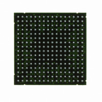
XC2V250-4FGG256C Xilinx Inc, XC2V250-4FGG256C Datasheet - Page 82

XC2V250-4FGG256C
Manufacturer Part Number
XC2V250-4FGG256C
Description
FPGA Virtex-II™ Family 250K Gates 3456 Cells 650MHz 0.15um/0.12um (CMOS) Technology 1.5V 256-Pin FBGA
Manufacturer
Xilinx Inc
Series
Virtex™-IIr
Datasheet
1.XC2V250-4FGG256C.pdf
(318 pages)
Specifications of XC2V250-4FGG256C
Package
256FBGA
Family Name
Virtex-IIÂ
Device Logic Units
3456
Device System Gates
250000
Number Of Registers
3072
Maximum Internal Frequency
650 MHz
Typical Operating Supply Voltage
1.5 V
Maximum Number Of User I/os
172
Ram Bits
442368
Number Of Labs/clbs
384
Total Ram Bits
442368
Number Of I /o
172
Number Of Gates
250000
Voltage - Supply
1.425 V ~ 1.575 V
Mounting Type
Surface Mount
Operating Temperature
0°C ~ 85°C
Package / Case
256-BGA
Lead Free Status / RoHS Status
Lead free / RoHS Compliant
Number Of Logic Elements/cells
-
Lead Free Status / RoHS Status
Lead free / RoHS Compliant
Other names
122-1352
Available stocks
Company
Part Number
Manufacturer
Quantity
Price
Company:
Part Number:
XC2V250-4FGG256C
Manufacturer:
IR
Quantity:
120
Company:
Part Number:
XC2V250-4FGG256C
Manufacturer:
XILINX
Quantity:
1 045
- Current page: 82 of 318
- Download datasheet (3Mb)
Global Clock Setup and Hold for LVTTL Standard, Without DCM
,
Table 37: Global Clock Setup and Hold for LVTTL Standard, Without DCM
DS031-3 (v3.5) November 5, 2007
Product Specification
Notes:
1. IFF = Input Flip-Flop or Latch
2. Setup time is measured relative to the Global Clock input signal with the fastest route and the lightest load. Hold time is measured
3. These values are parametrically measured.
Input Setup and Hold Time Relative to
Global Clock Input Signal for LVTTL
Standard.
For data input with different
standards, adjust the setup time delay
by the values shown in
Switching Characteristics Standard
Adjustments, page
Full Delay
Global Clock and IFF
relative to the Global Clock input signal with the slowest route and heaviest load.
(2)
Description
R
11.
(1)
IOB Input
without DCM
T
PSFD
Symbol
/T
PHFD
www.xilinx.com
Virtex-II Platform FPGAs: DC and Switching Characteristics
XC2V1000
XC2V1500
XC2V2000
XC2V3000
XC2V4000
XC2V6000
XC2V8000
XC2V250
XC2V500
XC2V40
XC2V80
Device
1.92/ 0.00
2.10/ 0.00
1.92/ 0.00
1.92/ 0.00
1.92/ 0.00
1.92/ 0.00
1.92/ 0.00
1.92/ 0.00
2.00/ 0.00
1.92/ 0.50
-6
Speed Grade
1.92/ 0.00
2.10/ 0.00
1.92/ 0.00
1.92/ 0.00
1.92/ 0.00
1.92/ 0.00
1.92/ 0.00
1.92/ 0.00
2.00/ 0.00
1.92/ 0.50
2.38/ 0.00
-5
2.21/ 0.00
2.21/ 0.00
2.21/ 0.00
2.21/ 0.00
2.21/ 0.00
2.21/ 0.00
2.21/ 0.00
2.21/ 0.00
2.30/ 0.00
2.21/ 0.50
2.60/ 0.00
-4
Module 3 of 4
Units
ns
ns
ns
ns
ns
ns
ns
ns
ns
ns
ns
34
Related parts for XC2V250-4FGG256C
Image
Part Number
Description
Manufacturer
Datasheet
Request
R

Part Number:
Description:
IC FPGA VIRTEX-II 250K 144-CSBGA
Manufacturer:
Xilinx Inc
Datasheet:

Part Number:
Description:
IC FPGA VIRTEX-II 250K 144-CSBGA
Manufacturer:
Xilinx Inc
Datasheet:

Part Number:
Description:
IC FPGA VIRTEX-II 250K 456-FBGA
Manufacturer:
Xilinx Inc
Datasheet:

Part Number:
Description:
IC FPGA VIRTEX-II 250K 256-FBGA
Manufacturer:
Xilinx Inc
Datasheet:

Part Number:
Description:
IC FPGA VIRTEX-II 250K 256-FBGA
Manufacturer:
Xilinx Inc
Datasheet:

Part Number:
Description:
IC FPGA VIRTEX-II 250K 144-CSBGA
Manufacturer:
Xilinx Inc
Datasheet:

Part Number:
Description:
IC FPGA VIRTEX-II 250K 144-CSBGA
Manufacturer:
Xilinx Inc
Datasheet:

Part Number:
Description:
IC FPGA VIRTEX-II 250K 456-FBGA
Manufacturer:
Xilinx Inc
Datasheet:

Part Number:
Description:
IC FPGA VIRTEX-II 250K 456-FBGA
Manufacturer:
Xilinx Inc
Datasheet:

Part Number:
Description:
IC FPGA VIRTEX-II 250K 256-FBGA
Manufacturer:
Xilinx Inc
Datasheet:

Part Number:
Description:
IC FPGA VIRTEX-II 250K 256-FBGA
Manufacturer:
Xilinx Inc
Datasheet:

Part Number:
Description:
IC FPGA VIRTEX-II 250K 456-FBGA
Manufacturer:
Xilinx Inc
Datasheet:

Part Number:
Description:
IC FPGA VIRTEX-II 250K 456-FBGA
Manufacturer:
Xilinx Inc
Datasheet:

Part Number:
Description:
IC FPGA VIRTEX-II 456FGBGA
Manufacturer:
Xilinx Inc
Datasheet:

Part Number:
Description:
IC FPGA VIRTEX-II 456FGBGA
Manufacturer:
Xilinx Inc
Datasheet:


