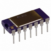
AD637KD Analog Devices Inc, AD637KD Datasheet - Page 11

AD637KD
Manufacturer Part Number
AD637KD
Description
RMS TO DC CONVERTER IC
Manufacturer
Analog Devices Inc
Datasheet
1.AD637JRZ.pdf
(20 pages)
Specifications of AD637KD
Rohs Status
RoHS non-compliant
Current - Supply
2.2mA
Voltage - Supply
±3.0V ~ 18V
Mounting Type
Through Hole
Package / Case
14-CDIP (0.300", 7.62mm)
Bandwidth
8MHz
Supply Current
2.2mA
Power Dissipation Pd
108mW
Supply Voltage Range
± 3V To ± 18V
Digital Ic Case Style
DIP
No. Of Pins
14
Operating Temperature Range
0°C To +70°C
For Use With
AD637-EVALZ - BOARD EVALUATION FOR AD637
Lead Free Status / RoHS Status
Available stocks
Company
Part Number
Manufacturer
Quantity
Price
B
Table 5. Practical Values of C
Input Waveform
and Period
A
C
D
FREQUENCY RESPONSE
The frequency response of the AD637 at various signal levels is
shown in Figure 15. The dashed lines show the upper frequency
limits for 1%, 10%, and ±3 dB of additional error. For example,
note that for 1% additional error with a 2 V rms input, the
highest frequency allowable is 200 kHz. A 200 mV signal can
be measured with 1% error at signal frequencies up to 100 kHz.
To take full advantage of the wide bandwidth of the AD637,
care must be taken in the selection of the input buffer amplifier.
To ensure that the input signal is accurately presented to the
converter, the input buffer must have a −3 dB bandwidth that is
wider than that of the AD637. Note the importance of slew rate
in this application. For example, the minimum slew rate required
for a 1 V rms, 5 MHz, sine wave input signal is 44 V/μs. The user is
cautioned that this is the minimum rising or falling slew rate
and that care must be exercised in the selection of the buffer
amplifier, because some amplifiers exhibit a two-to-one
difference between rising and falling slew rates. The AD845 is
recommended as a precision input buffer.
Sine Wave with dc Offset
Symmetrical Sine Wave
Pulse Train Waveform
T
T
T
T
T
T
2
2
0V
0V
0V
0V
Absolute Value
Circuit Waveform
and Period
T
T
T
AV
T
T
2
1/2T
2
and C2 for Various Input Waveforms
Minimum R × C
Time Constant
1/2T
T
10 (T − T
10 (T − 2T
2
)
2
)
Rev. K | Page 11 of 20
AV
0.82
6.8
5.6
C
0.47
AV
for 1% Averaging Error @ 60 Hz with T = 16.6 ms
Recommended Standard Values for C
(μF)
0.01
0.1
10
1
1k
100mV RMS INPUT
10mV RMS INPUT
7V RMS INPUT
2V RMS INPUT
1V RMS INPUT
Figure 15. Frequency Response
10k
C2 (μF)
1.5
2.7
22
18
INPUT FREQUENCY (Hz)
100k
AV
1%
and C2
10%
1M
±3dB
1% Settling
Time
181 ms
325 ms
2.67 sec
2.17 sec
AD637
10M


