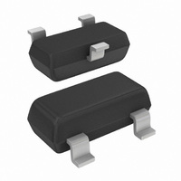
BFS17A,215 NXP Semiconductors, BFS17A,215 Datasheet - Page 2

BFS17A,215
Manufacturer Part Number
BFS17A,215
Description
TRANS NPN 25MA 15V 3GHZ SOT23
Manufacturer
NXP Semiconductors
Datasheet
1.BFS17A215.pdf
(9 pages)
Specifications of BFS17A,215
Package / Case
SOT-23-3, TO-236-3, Micro3™, SSD3, SST3
Transistor Type
NPN
Voltage - Collector Emitter Breakdown (max)
15V
Frequency - Transition
2.8GHz
Noise Figure (db Typ @ F)
2.5dB @ 800MHz
Power - Max
300mW
Dc Current Gain (hfe) (min) @ Ic, Vce
25 @ 2mA, 1V
Current - Collector (ic) (max)
25mA
Mounting Type
Surface Mount
Dc Current Gain Hfe Max
25 @ 2mA @ 1V
Mounting Style
SMD/SMT
Configuration
Single
Transistor Polarity
NPN
Maximum Operating Frequency
2800 MHz (Typ)
Collector- Emitter Voltage Vceo Max
15 V
Emitter- Base Voltage Vebo
2.5 V
Continuous Collector Current
0.025 A
Power Dissipation
300 mW
Maximum Operating Temperature
+ 150 C
Number Of Elements
1
Collector-emitter Voltage
15V
Collector-base Voltage
25V
Emitter-base Voltage
2.5V
Collector Current (dc) (max)
25mA
Dc Current Gain (min)
25
Frequency (max)
2.8GHz
Operating Temp Range
-65C to 150C
Operating Temperature Classification
Military
Mounting
Surface Mount
Pin Count
3
Package Type
TO-236AB
Lead Free Status / RoHS Status
Lead free / RoHS Compliant
Gain
-
Lead Free Status / Rohs Status
Lead free / RoHS Compliant
Other names
568-1653-2
933750250215
BFS17A T/R
933750250215
BFS17A T/R
NXP Semiconductors
DESCRIPTION
NPN transistor in a plastic SOT23 package.
APPLICATIONS
It is intended for RF applications such as oscillators
PINNING
QUICK REFERENCE DATA
LIMITING VALUES
In accordance with the Absolute Maximum Rating System (IEC 134).
Note to the Quick reference data and the Limiting values
1. T
September1995
V
V
I
P
f
G
F
V
V
V
V
I
I
P
T
T
SYMBOL
SYMBOL
C
T
C
CM
in TV tuners.
stg
j
CBO
CEO
tot
O
CBO
CEO
EBO
tot
NPN 3 GHz wideband transistor
UM
PIN
1
2
3
s
is the temperature at the soldering point of the collector pin.
base
emitter
collector
collector-base voltage
collector-emitter voltage
DC collector current
total power dissipation
transition frequency
maximum unilateral power gain
noise figure
output voltage
collector-base voltage
collector-emitter voltage
emitter-base voltage
DC collector current
peak collector current
total power dissipation
storage temperature
junction temperature
PARAMETER
PARAMETER
DESCRIPTION
open base
up to T
I
I
open base
open collector
up to T
open emitter
T
I
T
d
R
f
open emitter
C
C
C
(p+qr)
im
amb
amb
L
= 25 mA; V
= 14 mA; V
= 2 mA; V
= 75 ; T
= 60 dB; I
= 25 C
= 25 C
= 793.25 MHz
s
s
= 70 C; note 1
= 70 C; note 1
2
CONDITIONS
CE
CONDITIONS
amb
handbook, halfpage
CE
CE
C
= 5 V; f = 800 MHz;
Marking code: E2p.
= 14 mA; V
= 25 C;
= 5 V; f = 500 MHz;
= 10 V; f = 800 MHz
CE
= 10 V;
Top view
1
Fig.1 SOT23.
2.8
13.5
2.5
150
65
TYP.
MIN.
3
MSB003
Product specification
2
25
15
25
300
25
15
2.5
25
50
300
+150
150
MAX.
MAX.
BFS17A
V
V
mA
mW
GHz
dB
dB
mV
V
V
V
mA
mA
mW
C
C
UNIT
UNIT


