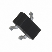
BF511,215 NXP Semiconductors, BF511,215 Datasheet - Page 3

BF511,215
Manufacturer Part Number
BF511,215
Description
JFET N-CHAN 20V SOT-23
Manufacturer
NXP Semiconductors
Datasheet
1.BF511215.pdf
(9 pages)
Specifications of BF511,215
Package / Case
SOT-23-3, TO-236-3, Micro3™, SSD3, SST3
Transistor Type
N-Channel JFET
Frequency
100MHz
Voltage - Rated
20V
Current Rating
30mA
Noise Figure
1.5dB
Current - Test
5mA
Voltage - Test
10V
Configuration
Single
Transistor Polarity
N-Channel
Drain Source Voltage Vds
20 V
Continuous Drain Current
30 mA
Maximum Operating Temperature
+ 150 C
Maximum Drain Gate Voltage
20 V
Mounting Style
SMD/SMT
Lead Free Status / RoHS Status
Lead free / RoHS Compliant
Power - Output
-
Gain
-
Lead Free Status / Rohs Status
Lead free / RoHS Compliant
Other names
568-1965-2
933505280215
BF511 T/R
933505280215
BF511 T/R
NXP Semiconductors
RATINGS
Limiting values in accordance with the Absolute Maximum System (IEC 134)
THERMAL RESISTANCE
Note
1. Mounted on a ceramic substrate of 8 mm 10 mm 0.7 mm.
STATIC CHARACTERISTICS
T
December 1997
Drain-source voltage
Drain-gate voltage (open source)
Drain current (DC or average)
Gate current
Total power dissipation up to T
Storage temperature range
Junction temperature
From junction to ambient (note 1)
Gate cut-off current
Gate-drain breakdown voltage
Drain current
Gate-source cut-off voltage
amb
N-channel silicon field-effect transistors
V
I
V
I
S
D
DS
= 25 C
= 0; I
= 10 A; V
GS
= 10 V; V
= 0.2 V; V
D
= 10 A
DS
GS
DS
= 10 V
= 0
= 0
amb
= 40 C (note 1)
I
V
I
V
DSS
GSS
(BR)GDO
(P)GS
<
typ.
3
BF510
0.7
3.0
0.8
10
20
511
R
V
V
I
I
P
T
T
D
2.5
7.0
1.5
stg
j
DS
DGO
tot
th j-a
10
20
G
512
2.2
10
20
12
=
max.
max.
max.
max.
max.
65 to 150 C
max.
6
BF510 to 513
Product specification
513
250 mW
150 C
430 K/W
20 V
20 V
30 mA
10 mA
10 nA
20 V
10
18
3 V
mA
mA


