J310 Fairchild Semiconductor, J310 Datasheet - Page 2
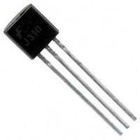
J310
Manufacturer Part Number
J310
Description
IC SWITCH RF N-CH 25V 10MA TO-92
Manufacturer
Fairchild Semiconductor
Datasheet
1.J310.pdf
(6 pages)
Specifications of J310
Transistor Type
N-Channel JFET
Frequency
450MHz
Gain
12dB
Voltage - Rated
25V
Current Rating
60mA
Noise Figure
3dB
Current - Test
10mA
Voltage - Test
10V
Package / Case
TO-92-3 (Standard Body), TO-226
Transistor Polarity
N-Channel
Forward Transconductance Gfs (max / Min)
0.008 S to 0.018 S
Drain Source Voltage Vds
25 V
Gate-source Cutoff Voltage
- 6.5 V
Gate-source Breakdown Voltage
- 25 V
Drain Current (idss At Vgs=0)
15 mA to 40 mA
Power Dissipation
625 mW
Maximum Operating Temperature
+ 150 C
Configuration
Single
Minimum Operating Temperature
- 55 C
Mounting Style
Through Hole
Breakdown Voltage Vbr
-25V
Zero Gate Voltage Drain Current Idss
24mA To 60mA
Gate-source Cutoff Voltage Vgs(off) Max
-6.5V
Power Dissipation Pd
350mW
Rohs Compliant
Yes
Lead Free Status / RoHS Status
Lead free / RoHS Compliant
Power - Output
-
Lead Free Status / Rohs Status
Lead free / RoHS Compliant
Available stocks
Company
Part Number
Manufacturer
Quantity
Price

Company:
Part Number:
J310
Manufacturer:
FAIRCHILD
Quantity:
65 000
Part Number:
J310
Manufacturer:
FAIRCHILD/仙童
Quantity:
20 000
Company:
Part Number:
J310 DZ
Manufacturer:
FAIRCHILD
Quantity:
10 750
Company:
Part Number:
J310G
Manufacturer:
ON Semiconductor
Quantity:
1 150
Company:
Part Number:
J310RLRP
Manufacturer:
MOTOROLA
Quantity:
18 000


J309 / J310 / MMBFJ309 / MMBFJ310 Rev. A1
© 2010 Fairchild Semiconductor Corporation
Electrical Characteristics
* Pulse Test: Pulse Width ≤ 300μs, Duty Cycle ≤ 2.0%
Off Characteristics
BV
On Characteristics
Small Signal Characteristics
Symbol
V
Re
Re
Re
Re
V
I
(BR)GSS
GS(off)
I
g
G
C
C
g
GSS
DSS
NF
GS(f)
g
g
e
oss
(yos)
(yfs
(yig)
og
(yis)
dg
pg
fs
fg
sg
n
)
Gate-Source Breakdown Voltage I
Gate Reverse Current
Gate-Source Cutoff Voltage
Zero-Gate Voltage Drain
Current*
Gate-Source Forward Voltage
Common-Source Input
Conductance
Common-Source Output
Conductance
Common-Gate Power Gain
Common-Source Forward
Transconductance
Common-Gate Input
Conductance
Common-Source Forward
Transconductance
Common-Source Output
Conductance
Common-Gate Forward
Conductance
Common-Gate Output
Conductance
Drain-Gate Capacitance
Source-Gate Capacitance
Noise Figure
Equivalent Short-Circuit Input
Noise Voltage
Parameter
T
a
= 25°C unless otherwise noted
V
V
V
V
V
V
V
V
V
V
V
V
V
V
V
V
V
V
G
GS
GS
DS
DS
DS
DS
DS
DS
DS
DS
DS
DS
DS
DS
DS
DS
DS
DS
= -1.0μA, V
= 10V, I
= 10V, V
= 0, I
= 10V, I
= 10V, I
= 10V, I
= 10V, I
= 10V, I
= 10V, I
= 10V, I
= 10V, I
= 10V, I
= 0, V
= 0, V
= 10V, I
= 10V, I
= -15V, V
= -15V, V
Test Condition
G
GS
GS
2
= 1.0mA
D
D
D
D
D
D
D
D
D
D
D
D
GS
DS
= -10V, f = 1.0MHz
= -10V, f = 1.0MHz
DS
DS
= 1.0nA
= 10mA, f = 100MHz
= 10mA, f = 100MHz
= 10mA, f = 100MHz
= 10mA, f = 100MHz
= 10mA, f = 100MHz
= 10mA, f = 1.0kHz
= 10mA, f = 1.0kHz
= 10mA, f = 1.0kHz
= 10mA, f = 1.0kHz
= 10mA, f = 450MHz
= 10mA, f = 100Hz
= 0
= 0
= 0
= 0, T
a
= 125°C
309
310
309
310
309
310
309
310
309
310
309
310
10,000
8,000
Min.
-1.0
-2.0
-25
12
24
13,000
12,000
Typ.
0.25
100
150
0.7
0.5
2.0
4.1
3.0
6.0
16
12
12
20,000
18,000
Max.
-1.0
-1.0
-4.0
-6.5
150
1.0
2.5
5.0
30
60
www.fairchildsemi.com
mmhos
mmhos
mmhos
mmhos
mmhos
μmhos
μmhos
μmhos
μmhos
μmhos
μmhos
μmhos
nV/ Hz
Units
mA
mA
nA
μA
dB
dB
pF
pF
V
V
V
V
Related parts for J310
Image
Part Number
Description
Manufacturer
Datasheet
Request
R

Part Number:
Description:
Fairchild Semiconductor [IGBT MODULE]
Manufacturer:
Fairchild Semiconductor
Datasheet:

Part Number:
Description:
Discrete Semiconductor Modules
Manufacturer:
Fairchild Semiconductor
Part Number:
Description:
Discrete Semiconductor Modules
Manufacturer:
Fairchild Semiconductor
Part Number:
Description:
This N-Channel MOSFET is produced using Fairchild Semiconductor’s advanced Power Trench® process
Manufacturer:
Fairchild Semiconductor
Datasheet:
Part Number:
Description:
This N-Channel MOSFET is produced using Fairchild Semiconductor’s advanced Power Trench® process
Manufacturer:
Fairchild Semiconductor
Datasheet:
Part Number:
Description:
This N-Channel MOSFET is produced using Fairchild Semiconductor’s advanced PowerTrench® process
Manufacturer:
Fairchild Semiconductor
Datasheet:
Part Number:
Description:
This N-Channel MOSFET is produced using Fairchild Semiconductor’s advanced PowerTrench® process
Manufacturer:
Fairchild Semiconductor
Datasheet:
Part Number:
Description:
This N-Channel MOSFET is produced using Fairchild Semiconductor’s advanced Power Trench® process
Manufacturer:
Fairchild Semiconductor
Datasheet:
Part Number:
Description:
This N-Channel logic Level MOSFETs are produced using Fairchild Semiconductor‘s advanced Power Trench® process that has been special tailored to minimize the on-state resistance and yet maintain superior switching performance
Manufacturer:
Fairchild Semiconductor
Datasheet:
Part Number:
Description:
This N-Channel MOSFET is produced using Fairchild Semiconductor’s advanced Power Trench® process
Manufacturer:
Fairchild Semiconductor
Datasheet:
Part Number:
Description:
This N-Channel SyncFET™ is produced using Fairchild Semiconductor’s advanced PowerTrench® process
Manufacturer:
Fairchild Semiconductor
Datasheet:
Part Number:
Description:
This N-Channel SyncFET™ is produced using Fairchild Semiconductor’s advanced PowerTrench® process
Manufacturer:
Fairchild Semiconductor
Datasheet:
Part Number:
Description:
This N-Channel SyncFET™ is produced using Fairchild Semiconductor’s advanced PowerTrench® process
Manufacturer:
Fairchild Semiconductor
Datasheet:
Part Number:
Description:
This N-Channel logic Level MOSFETs are produced using Fairchild Semiconductor‘s advanced Power Trench® process that has been special tailored to minimize the on-state resistance and yet maintain superior switching performance
Manufacturer:
Fairchild Semiconductor
Datasheet:
Part Number:
Description:
This N-Channel MOSFET is produced using Fairchild Semiconductor’s advanced Power Trench® process that has been especially tailored to minimize the on-state resistance and yet maintain superior switching performance
Manufacturer:
Fairchild Semiconductor
Datasheet: