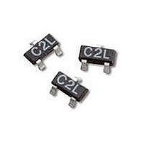
HSMS-281C-TR2G Avago Technologies US Inc., HSMS-281C-TR2G Datasheet - Page 6

HSMS-281C-TR2G
Manufacturer Part Number
HSMS-281C-TR2G
Description
DIODE SCHOTTKY GP LN 20V SOT-323
Manufacturer
Avago Technologies US Inc.
Datasheet
1.HSMS-281C-TR2G.pdf
(10 pages)
Specifications of HSMS-281C-TR2G
Package / Case
SC-70-3, SOT-323-3
Diode Type
Schottky - 1 Pair Series Connection
Voltage - Peak Reverse (max)
20V
Current - Max
1A
Capacitance @ Vr, F
1.2pF @ 0V, 1MHz
Resistance @ If, F
15 Ohm @ 5mA, 1MHz
Product
Schottky Diodes
Peak Reverse Voltage
20 V
Forward Continuous Current
1 A
Configuration
Dual Series
Forward Voltage Drop
410 mV
Maximum Reverse Leakage Current
0.2 uA at 15 V
Operating Temperature Range
+ 150 C
Mounting Style
SMD/SMT
Lead Free Status / RoHS Status
Lead free / RoHS Compliant
Power Dissipation (max)
-
Lead Free Status / RoHS Status
Lead free / RoHS Compliant, Lead free / RoHS Compliant
SMT Assembly
Reliable assembly of surface mount components is a com‑
plex process that involves many material, process, and
equipment factors, including: method of heating (e.g., IR
or vapor phase reflow, wave soldering, etc.) circuit board
material, conductor thickness and pattern, type of solder
alloy, and the thermal conductivity and thermal mass of
components. Components with a low mass, such as the
SOT package, will reach solder reflow temperatures faster
than those with a greater mass.
Avago’s SOT diodes have been qualified to the time‑tem‑
perature profile shown in Figure 8. This profile is repre‑
sentative of an IR reflow type of surface mount assembly
process.
After ramping up from room temperature, the circuit
board with components attached to it (held in place with
solder paste) passes through one or more preheat zones.
Figure 8. Surface Mount Assembly Profile.
Lead-Free Reflow Profile Recommendation (IPC/JEDEC J-STD-020C)
Note 1: All temperatures refer to topside of the package, measured on the package body surface
6
Reflow Parameter
Average ramp‑up rate (Liquidus Temperature (T
Preheat
Ts(max) to TL Ramp‑up Rate
Time maintained above:
Peak Temperature (T
Time within 5 °C of actual Peak temperature (t
Ramp‑down Rate
Time 25 °C to Peak Temperature
Tp
T
25
L
Ts
Ts
min
max
P
)
t 25
Preheat
°
ts
C to Peak
P
)
Ramp-up
S(max)
Time
to Peak)
Temperature Min (T
Temperature Max (T
Time (min to max) (t
Temperature (T
Time (t
Ramp-down
tp
The preheat zones increase the temperature of the board
and components to prevent thermal shock and begin
evaporating solvents from the solder paste. The reflow
zone briefly elevates the temperature sufficiently to pro‑
duce a reflow of the solder.
The rates of change of temperature for the ramp‑up and
cool‑down zones are chosen to be low enough to not
cause deformation of the board or damage to compo‑
nents due to thermal shock. The maximum temperature
in the reflow zone (T
These parameters are typical for a surface mount assem‑
bly process for Avago diodes. As a general guideline, the
circuit board and components should be exposed only
to the minimum temperatures and times necessary to
achieve a uniform reflow of solder.
L
t
)
L
L
)
S(min)
S(max)
S
)
Critical Zone
T
L
)
to Tp
)
MAX
) should not exceed 260°C.
Lead-Free Assembly
3°C/ second max
150°C
200°C
60‑180 seconds
3°C/second max
217°C
60‑150 seconds
260 +0/‑5°C
20‑40 seconds
6°C/second max
8 minutes max


