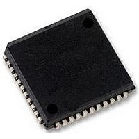
SCC68681C1A44 NXP Semiconductors, SCC68681C1A44 Datasheet - Page 15

SCC68681C1A44
Manufacturer Part Number
SCC68681C1A44
Description
UART 2-CH 5V 44-Pin PLCC Tube
Manufacturer
NXP Semiconductors
Datasheet
1.SCC68681C1A44512.pdf
(29 pages)
Specifications of SCC68681C1A44
Package
44PLCC
Number Of Channels Per Chip
2
Maximum Data Rate
0.1152 MBd
Transmitter And Receiver Fifo Counter
No
Operating Supply Voltage
5 V
Minimum Single Supply Voltage
4.5 V
Maximum Processing Temperature
260 °C
Maximum Supply Current
10 mA
No. Of Channels
2
Uart Features
Quadruple Buffered Receiver Data Register
Supply Voltage Range
4.5V To 5.5V
Operating Temperature Range
0°C To +70°C
Digital Ic Case Style
PLCC
No. Of Pins
44
Data Rate
115.2Kilobaud
Rohs Compliant
Yes
Lead Free Status / RoHS Status
Lead free / RoHS Compliant
Available stocks
Company
Part Number
Manufacturer
Quantity
Price
Company:
Part Number:
SCC68681C1A44
Manufacturer:
FREESCALE
Quantity:
1 596
Company:
Part Number:
SCC68681C1A44
Manufacturer:
PHI
Quantity:
5 530
Company:
Part Number:
SCC68681C1A44
Manufacturer:
PH
Quantity:
504
Part Number:
SCC68681C1A44
Manufacturer:
NXP/恩智浦
Quantity:
20 000
Company:
Part Number:
SCC68681C1A44,512
Manufacturer:
NXP Semiconductors
Quantity:
10 000
Company:
Part Number:
SCC68681C1A44,518
Manufacturer:
NXP Semiconductors
Quantity:
10 000
Company:
Part Number:
SCC68681C1A44,529
Manufacturer:
NXP Semiconductors
Quantity:
10 000
Company:
Part Number:
SCC68681C1A44529
Manufacturer:
NXP Semiconductors
Quantity:
135
Philips Semiconductors
OPCR – Output Port Configuration Register
OPCR[7] – OP7 Output Select
This bit programs the OP7 output to provide one of the following:
0: The complement of OPR[7].
1: The Channel B transmitter interrupt output which is the comple-
OPCR[6] – OP6 Output Select
This bit programs the OP6 output to provide one of the following:
0: The complement of OPR[6].
1: The Channel A transmitter interrupt output which is the comple-
OPCR[5] – OP5 Output Select
This bit programs the OP5 output to provide one of the following:
0: The complement of OPR[5].
1: The Channel B transmitter interrupt output which is the comple-
OPCR[4] – OP4 Output Select
This field programs the OP4 output to provide one of the following:
0: The complement of OPR[4].
1: The Channel A receiver interrupt output which is the comple-
OPCR[3:2] – OP3 Output Select
This bit programs the OP3 output to provide one of the following:
00: The complement of OPR[3].
01: The counter/timer output, in which case OP3 acts as an open-
10: The 1 clock for the Channel B transmitter, which is the clock
11: The 1 clock for the Channel B receiver, which is the clock that
OPCR[1:0] – OP2 Output Select
This field programs the OP2 output to provide one of the following:
00: The complement of OPR[2].
01: The 16 clock for the Channel A transmitter. This is the clock
2004 Apr 06
Dual asynchronous receiver/transmitter (DUART)
ment of TxRDYB. When in this mode OP7 acts as an open-
drain output. Note that this output is not masked by the contents
of the IMR.
ment of TxRDYA. When in this mode OP6 acts as an open-
drain output. Note that this output is not masked by the contents
of the IMR.
ment of ISR[5]. When in this mode OP5 acts as an open-drain
output. Note that this output is not masked by the contents of
the IMR.
ment of ISR[1]. When in this mode OP4 acts as an open-drain
output. Note that this output is not masked by the contents of
the IMR.
drain output. In the timer mode, this output is a square wave at
the programmed frequency. In the counter mode, the output
remains HIGH until terminal count is reached, at which time it
goes LOW. The output returns to the HIGH state when the
counter is stopped by a stop counter command. Note that this
output is not masked by the contents of the IMR.
that shifts the transmitted data. If data is not being transmitted,
a free running 1 clock is output.
samples the received data. If data is not being received, a free
running 1 clock is output.
selected by CSRA[3:0], and will be a 1 clock if CSRA[3:0] = 1111.
15
of 4.1% to 6.7% in a ‘clean’ communications channel. The percent of
Duty cycle of 16 clock is 50%
Rates will change in direct proportion to to the X1 rate of 3.6864 MHz.
10: The 1 clock for the Channel A transmitter, which is the clock
11: The 1 clock for the Channel A receiver, which is the clock that
Table 4.
NOTE:
Asynchronous UART communications can tolerate frequency error
error changes as the character length changes. The above
percentages range from 5 bits not parity to 8 bits with parity and one
stop bit. The error with 8 bits not parity and one stop bit is 4.6%. If a
stop bit length of 9/16 is used, the error tolerance will approach 0
due to a variable error of up to 1/16 bit time in receiver clock phase
alignment to the start bit.
NORMAL RATE
that shifts the transmitted data. If data is not being transmitted,
a free running 1 clock is output.
samples the received data. If data is not being received, a free
running 1 clock is output.
(BAUD)
115.2 k
14.4 k
19.2 k
28.8 k
38.4 k
57.6 k
134.5
1050
1200
1800
2000
2400
4800
7200
9600
150
200
300
600
110
50
75
Bit Rate Generator Characteristics
Crystal or Clock = 3.6864MHz
CLOCK (kHz)
ACTUAL 16
1843.2 k
16.756
32.056
1.759
2.153
153.6
230.4
307.2
460.8
614.4
921.6
115.2
1%.
19.2
28.8
38.4
76.8
0.8
1.2
2.4
3.2
4.8
9.6
SCC68681
ERROR (%)
–0.069
–0.260
0.059
0.175
Product data
0
0
0
0
0
0
0
0
0
0
0
0
0
0
0
0
0
0


