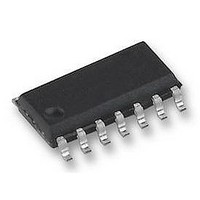
74HC4066D NXP Semiconductors, 74HC4066D Datasheet - Page 11

74HC4066D
Manufacturer Part Number
74HC4066D
Description
Analog Switch Quad SPST 14-Pin SO Bulk
Manufacturer
NXP Semiconductors
Type
Analog Switchr
Datasheet
1.74HC4066PW118.pdf
(27 pages)
Specifications of 74HC4066D
Package
14SO
Maximum On Resistance
142@4.5V Ohm
Maximum Propagation Delay Bus To Bus
8(Typ)@2V|3(Typ)@4.5V|2(Typ)@6V|2(Typ)@9V ns
Maximum Low Level Output Current
25 mA
Maximum Turn-off Time
44(Typ)@2V ns
Maximum Turn-on Time
36(Typ)@2V ns
Switch Architecture
SPST
Power Supply Type
Single
No. Of Channels
4
Turn Off Time
13ns
Turn On Time
11ns
Supply Voltage Range
2V To 10V
Operating Temperature Range
-40°C To +125°C
Analogue Switch Case Style
SOIC
No. Of Pins
14
Svhc
No SVHC
Analogue Switch Type
Bilateral
On State Resistance Max
105ohm
Rohs Compliant
Yes
Analog Switch Type
SPST
Dc
0722
Lead Free Status / RoHS Status
Lead free / RoHS Compliant
Available stocks
Company
Part Number
Manufacturer
Quantity
Price
Part Number:
74HC4066D
Manufacturer:
TI
Quantity:
20 000
Part Number:
74HC4066DB
Manufacturer:
PHILIPS/飞利浦
Quantity:
20 000
Company:
Part Number:
74HC4066DB118
Manufacturer:
NXP Semiconductors
Quantity:
1 996
Philips Semiconductors
Resistance R
For 74HC4066: V
or nZ, whichever is assigned as an input; see Fig.9.
Notes
1. At supply voltages approaching 2 V, the analog ON-resistance switch becomes extremely non-linear. Therefore, it is
2. All typical values are measured at T
2004 Nov 11
T
R
R
T
R
R
SYMBOL
amb
R
amb
ON(peak)
ON(rail)
ON(peak)
ON(rail)
Quad bilateral switches
ON
recommended that these devices are being used to transmit digital signals only, when using these supply voltages.
= 40 C to +85 C; note 2
= 40 C to +125 C
ON
ON-resistance
(peak)
ON-resistance
(rail)
maximum
variation of
ON-resistance
between any two
channels
ON-resistance
(peak)
ON-resistance
(rail)
PARAMETER
for 74HC4066 and 74HCT4066
CC
= 2.0, 4.5, 6.0 and 9.0 V; for 74HCT4066: V
V
V
V
V
V
V
V
I
I
I
I
I
I
I
= V
= V
= V
= V
= V
= V
= V
amb
IH
IH
IH
IH
IH
IH
IH
or V
or V
or V
or V
or V
or V
or V
= 25 C.
IL
IL
IL
IL
IL
IL
IL
OTHER
; V
; V
; V
; V
; V
; V
; V
is
is
is
is
is
is
is
TEST CONDITIONS
= V
= GND
= V
= V
= V
= GND
= V
CC
CC
CC
CC
CC
11
to GND
to GND
to GND
CC
= 4.5 V; note 1; V
100
1000
100
1000
100
1000
100
1000
100
1000
100
1000
I
S
( A)
74HC4066; 74HCT4066
2.0
4.5
6.0
9.0
2.0
4.5
6.0
9.0
2.0
4.5
6.0
9.0
2.0
4.5
6.0
9.0
2.0
4.5
6.0
9.0
2.0
4.5
6.0
9.0
2.0
4.5
6.0
9.0
V
CC
is
(V)
is the input voltage at pins nY
MIN.
Product specification
54
42
32
80
35
27
20
100
42
35
27
5
4
3
TYP. MAX. UNIT
118
105
88
95
82
70
106
94
78
142
126
105
115
100
85
128
113
95


