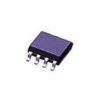
DG642DY Vishay, DG642DY Datasheet - Page 8

DG642DY
Manufacturer Part Number
DG642DY
Description
Video Switch ICs SPDT Analog Switch
Manufacturer
Vishay
Datasheet
1.DG642DJ-E3.pdf
(11 pages)
Specifications of DG642DY
Number Of Switches
Single
On Resistance (max)
8 Ohms
On Time (max)
100 ns
Off Time (max)
60 ns
Supply Voltage (max)
21 V
Maximum Operating Temperature
+ 85 C
Minimum Operating Temperature
- 40 C
Package / Case
SOIC-8 Narrow
Maximum Power Dissipation
300 mW
Mounting Style
SMD/SMT
Supply Current
3.5 mA
Switch Configuration
SPDT
Lead Free Status / RoHS Status
Lead free / RoHS Compliant
Available stocks
Company
Part Number
Manufacturer
Quantity
Price
Part Number:
DG642DY
Manufacturer:
EL
Quantity:
20 000
Company:
Part Number:
DG642DY-T1-E3
Manufacturer:
MINI
Quantity:
300
DG641, DG642, DG643
Vishay Siliconix
TEST CIRCUITS
APPLICATIONS
Device Description
The DG641, DG642, DG643 switches offer true bidirectional
switching of high frequency analog or digital signals with
minimum signal crosstalk, low insertion loss, and negligible
non-linearity distortion and group delay.
Built on the Siliconix D/CMOS process, these switches
provide excellent off-isolation with a bandwidth of around
500 MHz. The silicon-gate D/CMOS processing also yields
fast switching speeds.
An on-chip regulator circuit maintains TTL input compatibility
over the whole operating supply voltage range shown,
easing control logic interfacing.
Circuit layout is facilitated by the interchangeability of source
and drain terminals.
Frequency Response
A single switch on-channel exhibits both resistance [R
and capacitance [C
attenuation effect on the analog signal - which is frequency
dependent (like an RC low-pass filter). The - 3 dB bandwidth
of the DG641, DG642, DG643 is typically 500 MHz (into
50 ).
Power Supplies
Power supply flexibility is a useful feature of the DG641,
DG642, DG643 series. It can be operated from a single
positive supply (V+) if required (V- connected to ground).
Note that the analog signal must not exceed V- by more than
- 0.3 V to prevent forward biasing the substrate p-n junction.
The use of a V- supply has a number of advantages:
1.
www.vishay.com
8
It allows flexibility in analog signal handling, i.e., with
V- = - 5 V and V+ = 12 V; up to ± 5 V ac signals can
be controlled.
S(on)
]. This RC combination has an
Generator
Signal
50
DS(on)
Figure 6. Bandwidth
S
]
V-
2.
3.
Decoupling
It is an established rf design practice to incorporate sufficient
bypass capacitors in the circuit to decouple the power
supplies to all active devices in the circuit. The dynamic
performance of the DG641, DG642, DG643 series is
adversely affected by poor decoupling of power supply pins.
Also, of even more significance, since the substrate of the
device is connected to the negative supply, adequate
decoupling of this pin is essential. Suitable decoupling
capacitors are 1- to 10 µF tantalum bead, plus 10- to 100-nF
ceramic or polyester.
Rules:
1.
2.
3.
V+
- 3 V
D
+ 15 V
The value of on capacitance [C
A property known as ‘the body-effect’ on the DMOS
switch devices causes various parametric effects to
occur. One of these effects is the reduction in C
for an increasing V body-source. Note however that
to increase V- normally requires V+ to be reduced
(since V+ to V- = 21 V max.). A reduction in V+
causes an increase in r
has to be achieved. It is also useful to note that tests
indicate that optimum video linearity performance
(e.g., differential phase and gain) occurs when V- is
around - 3 V.
V- eliminates the need to bias the analog signal using
potential dividers and large coupling capacitors.
Decoupling capacitors should be incorporated on all
power supply pins (V+, V-). (see figure 7).
They should be mounted as close as possible to the
device pins.
Capacitors should be of a suitable type with good high
frequency characteristics - tantalum bead and/or
ceramic disc types are adequate.
50
R
L
V
OUT
DS(on)
S11-0154-Rev. F, 31-Jan-11
Document Number: 70058
, hence a compromise
S(on)
] may be reduced.
S(on)


