MC100LVEL34D ON Semiconductor, MC100LVEL34D Datasheet
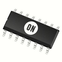
Clock Generators & Support Products 3.3V ECL Clock

MC100LVEL34D

Manufacturer Part Number
MC100LVEL34D
Description
Clock Generators & Support Products 3.3V ECL Clock
Manufacturer
ON Semiconductor
Datasheet

Specifications of MC100LVEL34D

Mounting Style
SMD/SMT
Package / Case
SOIC-16
Lead Free Status / RoHS Status
Lead free / RoHS Compliant

Available stocks

Company
Part Number
Manufacturer
Quantity
Price
Part Number:
MC100LVEL34DG
Manufacturer:
ON Semiconductor
Quantity:
135
Part Number:
MC100LVEL34DG
Manufacturer:
ON Semiconductor
Quantity:
114
Part Number:
MC100LVEL34DR2G
Manufacturer:
ON/安森美
Quantity:
20 000
MC100LVEL34
3.3V ECL ÷ 2, ÷ 4, ÷ 8 Clock
Generation Chip
Description
chip designed explicitly for low skew clock generation applications.
The internal dividers are synchronous to each other, therefore, the
common output edges are all precisely aligned. The V
internally generated voltage supply, is available to this device only.
For single−ended input conditions, the unused differential input is
connected to V
rebias AC coupled inputs. When used, decouple V
0.01 mF capacitor and limit current sourcing or sinking to 0.5 mA.
When not used, V
dividers will only be enabled/disabled when the internal clock is
already in the LOW state. This avoids any chance of generating a runt
clock pulse on the internal clock when the device is enabled/disabled
as can happen with an asynchronous control. An internal runt pulse
could lead to losing synchronization between the internal divider
stages. The internal enable flip-flop is clocked on the falling edge of
the input clock; therefore, all associated specification limits are
referenced to the negative edge of the clock input.
master reset (MR) input allows for the synchronization of the internal
dividers, as well as multiple LVEL34s in a system.
Features
© Semiconductor Components Industries, LLC, 2006
November, 2006 − Rev. 2
The MC100LVEL34 is a low skew ÷ 2, ÷ 4, ÷ 8 clock generation
The common enable (EN) is synchronous so that the internal
Upon start−up, the internal flip-flops will attain a random state; the
50 ps Typical Output-to-Output Skew
Synchronous Enable/Disable
Master Reset for Synchronization
1.5 GHz Toggle Frequency
The 100 Series Contains Temperature Compensation.
PECL Mode Operating Range:
NECL Mode Operating Range:
Open Input Default State
LVDS Input Compatible
Pb−Free Packages are Available
V
V
CC
CC
= 3.0 V to 3.8 V with V
= 0 V with V
BB
BB
as a switching reference voltage. V
should be left open.
EE
= −3.0 V to −3.8 V
EE
= 0 V
BB
and V
BB
BB
may also
1
CC
pin, an
via a
See detailed ordering and shipping information in the package
dimensions section on page 7 of this data sheet.
16
*For additional marking information, refer to
16
Application Note AND8002/D.
CASE 751B
(Note: Microdot may be in either location)
CASE 948F
DT SUFFIX
TSSOP−16
D SUFFIX
SO−16
ORDERING INFORMATION
A
L, WL
Y
W, WW = Work Week
G or G
1
1
http://onsemi.com
= Assembly Location
= Wafer Lot
= Year
= Pb−Free Package
Publication Order Number:
16
1
DIAGRAMS*
16
100LVEL34G
1
MARKING
AWLYWW
MC100LVEL34/D
ALYW G
VL34
100
G

Related parts for MC100LVEL34D

MC100LVEL34D Summary of contents

Page 1

MC100LVEL34 3.3V ECL ÷ 2, ÷ 4, ÷ 8 Clock Generation Chip Description The MC100LVEL34 is a low skew ÷ 2, ÷ 4, ÷ 8 clock generation chip designed explicitly for low skew clock generation applications. The internal dividers are ...

Page 2

÷ ÷ ÷ Warning: All V and V pins must be externally connected ...

Page 3

Table 4. MAXIMUM RATINGS Symbol Parameter V PECL Mode Power Supply CC V NECL Mode Power Supply EE V PECL Mode Input Voltage I NECL Mode Input Voltage I Output Current out I V Sink/Source Operating Temperature ...

Page 4

Table 6. 100LVEL DC CHARACTERISTICS, NECL Symbol Characteristic I Power Supply Current EE I Power Supply Current EE V Output HIGH Voltage (Note Output LOW Voltage (Note Input HIGH Voltage (Single−Ended Input ...

Page 5

There are two distinct functional relationships between the Master Reset and Clock: MR CLK CASE 1: If the MR is deasserted (H−L), while the Clock is still high, the outputs will follow the second ensuing clock ...

Page 6

JITTER OUT 100 0 0 500 FREQUENCY (MHz) Figure Driver Device Figure 5. Typical Termination for Output Driver ...

Page 7

... ORDERING INFORMATION Device MC100LVEL34D MC100LVEL34DG MC100LVEL34DR2 MC100LVEL34DR2G MC100LVEL34DT MC100LVEL34DTG MC100LVEL34DTR2 MC100LVEL34DTR2G †For information on tape and reel specifications, including part orientation and tape sizes, please refer to our Tape and Reel Packaging Specifications Brochure, BRD8011/D. *This package is inherently Pb−Free. Resource Reference of Application Notes ...

Page 8

G K −T− SEATING PLANE 0.25 (0.010 PACKAGE DIMENSIONS SO−16 D SUFFIX CASE 751B−05 ISSUE J −B− 0.25 (0.010 ...

Page 9

... −V− C 0.10 (0.004) −T− SEATING D PLANE 16X 0.36 *For additional information on our Pb−Free strategy and soldering details, please download the ON Semiconductor Soldering and Mounting Techniques Reference Manual, SOLDERRM/D. PACKAGE DIMENSIONS TSSOP−16 CASE 948F−01 ISSUE Ç Ç Ç ...

Page 10

... Opportunity/Affirmative Action Employer. This literature is subject to all applicable copyright laws and is not for resale in any manner. PUBLICATION ORDERING INFORMATION LITERATURE FULFILLMENT: Literature Distribution Center for ON Semiconductor P.O. Box 5163, Denver, Colorado 80217 USA Phone: 303−675−2175 or 800−344−3860 Toll Free USA/Canada Fax: 303− ...

Related keywords