E-TDA7461ND STMicroelectronics, E-TDA7461ND Datasheet
E-TDA7461ND
Specifications of E-TDA7461ND
Available stocks


Related parts for E-TDA7461ND


E-TDA7461ND Summary of contents
Page 1
... Device summary Order code TDA7461ND TDA7461NDTR (1) E-TDA7461ND (1) E-TDA7461NDTR 1. Device in ECOPACK® package, see January 2009 This is information on a product still in production but not recommended for new designs. Switched-capacitors design technique allows to obtain all these features without external components or adjustments. This means that higher quality and reliability walks alongside an overall cost saving ...
Page 2
... Pin description . . . . . . . . . . . . . . . . . . . . . . . . . . . . . . . . . . . . . . . . . . . . . . 6 2 Electrical specification . . . . . . . . . . . . . . . . . . . . . . . . . . . . . . . . . . . . . . . 8 2.1 Absolute maximum ratings . . . . . . . . . . . . . . . . . . . . . . . . . . . . . . . . . . . . . 8 2.2 Supply . . . . . . . . . . . . . . . . . . . . . . . . . . . . . . . . . . . . . . . . . . . . . . . . . . . . 8 2.3 ESD . . . . . . . . . . . . . . . . . . . . . . . . . . . . . . . . . . . . . . . . . . . . . . . . . . . . . . 8 2.4 Thermal data . . . . . . . . . . . . . . . . . . . . . . . . . . . . . . . . . . . . . . . . . . . . . . . 8 2.5 Audio processor part feature . . . . . . . . . . . . . . . . . . . . . . . . . . . . . . . . . . . 9 2.5.1 2.5.2 2.5.3 2.5.4 2.5.5 2.5.6 2.6 Audio processor electrical characteristics . . . . . . . . . . . . . . . . . . . . . . . . 10 3 Description of the audio processor part . . . . . . . . . . . . . . . . . . . . . . . . 13 3.1 Programmable input matrix . . . . . . . . . . . . . . . . . . . . . . . . . . . . . . . . . . . 13 3 ...
Page 3
... Data byte specification . . . . . . . . . . . . . . . . . . . . . . . . . . . . . . . . . . . . . . 35 7 Package information . . . . . . . . . . . . . . . . . . . . . . . . . . . . . . . . . . . . . . . . 46 8 Revision history . . . . . . . . . . . . . . . . . . . . . . . . . . . . . . . . . . . . . . . . . . . 47 Stereo decoder mute . . . . . . . . . . . . . . . . . . . . . . . . . . . . . . . . . . . . . . . 26 Input stages . . . . . . . . . . . . . . . . . . . . . . . . . . . . . . . . . . . . . . . . . . . . . . 26 Demodulator . . . . . . . . . . . . . . . . . . . . . . . . . . . . . . . . . . . . . . . . . . . . . 27 De-emphasis and high cut . . . . . . . . . . . . . . . . . . . . . . . . . . . . . . . . . . . 27 PLL and pilot tone detector . . . . . . . . . . . . . . . . . . . . . . . . . . . . . . . . . . 27 Fieldstrength control . . . . . . . . . . . . . . . . . . . . . . . . . . . . . . . . . . . . . . . 28 Level input and gain . . . . . . . . . . . . . . . . . . . . . . . . . . . . . . . . . . . . . . . . 28 Stereo blend control . . . . . . . . . . . . . . . . . . . . . . . . . . . . . . . . . . . . . . . . 28 High cut control . . . . . . . . . . . . . . . . . . . . . . . . . . . . . . . . . . . . . . . . . . . 29 Trigger path . . . . . . . . . . . . . . . . . . . . . . . . . . . . . . . . . . . . . . . . . . . . . . 30 Automatic noise controlled threshold adjustment (ATC Automatic threshold control ...
Page 4
... Table 6. Audio processor electrical characteristics Table 7. Input and source programming . . . . . . . . . . . . . . . . . . . . . . . . . . . . . . . . . . . . . . . . . . . . . . 14 Table 8. Stereo decoder electrical characteristics . . . . . . . . . . . . . . . . . . . . . . . . . . . . . . . . . . . . . . 20 Table 9. Noise blanker electrical characteristics Table 10. Multipath detector electrical characteristics . . . . . . . . . . . . . . . . . . . . . . . . . . . . . . . . . . . . 25 Table 11. Transmitted data (send mode Table 12. Subaddress (receive mode Table 13. Input selector . . . . . . . . . . . . . . . . . . . . . . . . . . . . . . . . . . . . . . . . . . . . . . . . . . . . . . . . . . . 35 Table 14. Loudness . . . . . . . . . . . . . . . . . . . . . . . . . . . . . . . . . . . . . . . . . . . . . . . . . . . . . . . . . . . . . . 36 Table 15. ...
Page 5
... Soft step timing . . . . . . . . . . . . . . . . . . . . . . . . . . . . . . . . . . . . . . . . . . . . . . . . . . . . . . . . . . 18 Figure 10. Bass control @ Hz Figure 11. Bass center @ Gain = 14 dB Figure 12. Bass quality factors @ Gain = 14 dB Figure 13. Bass normal and DC mode @ Gain = 14 dB Figure 14. Treble control @ fc = 17.5 kHz Figure 15. Treble center frequencies @ Gain = Figure 16. Noise blanker diagram . . . . . . . . . . . . . . . . . . . . . . . . . . . . . . . . . . . . . . . . . . . . . . . . . . . . 24 Figure 17. Trigger threshold vs. VPEAK . . . . . . . . . . . . . . . . . . . . . . . . . . . . . . . . . . . . . . . . . . . . . . . 24 Figure 18 ...
Page 6
... Block diagram and pin description 1 Block diagram and pin description 1.1 Block diagram Figure 1. Block diagram CDL CDG CDR MIXING AM STAGE 3 CASS R 4 CASS L INPUT PHONE MULTIPLEXER + 9 BEEP PHONE AUTO ZERO 8 PH GND PILOT 11 80KHz CANCELLATION MPX SUPPLY PLL 20 26 GND CREF 1 ...
Page 7
... CD right channel input CD left channel input AM input FM input (MPX) Level input stereo decoder Multipath detector input Multiplexer output left channel (stereo decoder output left (1) selectable Multiplexer output right channel (stereo decoder output right (1)) selectable Soft mute drive clock line data line ...
Page 8
... Table 4. Supply Symbol Parameter V Supply voltage S I Supply current S SVRR Ripple rejection @ 1 kHz 2.3 ESD All pins are protected against ESD according to the MIL883 standard. 2.4 Thermal data Table 5. Thermal data Symbol R Thermal resistance junction to pins th j-pins 8/48 Parameter Test condition ...
Page 9
... Treble control nd ● 2 order frequency response ● Center frequency programmable in 4 steps ● steps 2.5.5 Speaker control 4 independent speaker controls (1 dB steps control range 50 dB) 2.5.6 Mute function ● Direct mute ● Digitally controlled softmute with 4 programmable time constants Electrical specification 9/48 ...
Page 10
... Higher beep frequency BMAX Mixing control M Mixing level LEVEL Volume control G Max gain MAX A Max attenuation MAX 10/ kΩ; all gains = 0 dB kHz; unless otherwise specified). L Test condition all inputs except phone Adjacent gain step MIN MAX Differential Common mode kHz ...
Page 11
... THhigh R Internal pull-up resistor PU V Pull-up voltage PU Soft step T Switch time SW Bass control C Control range RANGE A Step resolution STEP f Center frequency C Q Quality factor BASS = 10 kΩ; all gains = 0 dB kHz; unless otherwise specified). L Test condition Adjacent attenuation steps From GMIN ( ...
Page 12
... S/N Signal to noise ratio d Distortion S Channel separation left/right C E Total tracking error T 1. The SM pin is active low (Mute = 0) 2. See description of audioprocessor part - bass & treble filter characteristics programming 12/ kΩ; all gains = 0 dB kHz; unless otherwise specified). L Test condition DC = off ...
Page 13
... The following picture shows the input and source programming flow: Figure 3. Input configuration tree APPL CASSETTE FM STD AM MONO PHONE ( AMSTD configuration the AM mono signal is lead through the FM stereo decoder part to use its additional filters. TDA7461 CD QD APPL. 2 APPL. 3 APPL ...
Page 14
... For example in Appl. 6 the TDA7461 has to be configured while startup with the data byte 0/xxxx0xxx. To select the FM phone source the last five significant bits of subaddress 0 have to be changed, for any other source the last three bits are sufficient (see data byte specification) ...
Page 15
... TDA7461 The TDA7461 can be configured with an additional input; if the AC coupling before the speaker stage is not used (bit 7 in subaddress 5 set to "1") ACINL and ACINR pins can be used as an additional stereo input. Figure 4. Input stages CD CDGND PHONE PH_GND CASSETTE AM MPX 3.1.3 AutoZero ...
Page 16
... Description of the audio processor part If bit D3 byte 10 (Stdec Register) is set to 0, then the stdec signal will be always available at the Mux out pins, no matter which is the selected source. The selection of the stereodecoder input, via a special procedure, is recommended. 1. Soft Mute or Mute the signal path 2 ...
Page 17
... For timing purposes the Bit 3 of the I the start of muting until the end of demuting. Figure 8. Softmute timing 1. Please notice that a started Mute action is always terminated and could not be interrupted by a change of the mute signal. 3.3.3 Soft step volume When volume level is changed often an audible click appears at the output. The root cause of those clicks could be either a DC offset before the volume stage or the sudden change of the envelope of the audio signal ...
Page 18
... Description of the audio processor part Figure 9. Soft step timing 1. For steps more than 1dB the soft step mode should be deactivated because it could generate a 1dB error during the blend-time. 3.3.4 Bass There are three parameters programmable in the bass stage (see ● Attenuation ● ...
Page 19
... Figure 12. Bass quality factors @ Gain = 14 dB Figure 14. Treble control @ fc = 17.5 kHz) (1) In general the center frequency, Q and DC-mode can be set independently. The exception from this rule is the mode (5/xx1111xx) where the center frequency is set to 150Hz instead of 100 Hz. Description of the audio processor part Figure 11 ...
Page 20
... Very high suppression of intermodulation and interference ● Programmable roll-off compensation ● Dedicated RDS Softmute ● High cut and stereo blend characteristics programmable in a wide range ● Internal Noise blanker with threshold controls ● Multipath detector with programmable internal/external influence 2 ● ...
Page 21
... Carrier and harmonic suppression at the output α19 Pilot signal α38 Sub carrier α57 Sub carrier α76 Sub carrier (2) Intermodulation ) α2 Pilot signal α3 = 500 mV, 75 kHz deviation kHz. MPX Test condition Min. Bit = 7, Subadr >> V LEVEL HCH Bit = 7, Subadr >> V LEVEL HCH Bit = 7, Subadr ...
Page 22
... By design/characterization but functionally guaranteed through dedicated test mode structure 2. Intermodulation Suppression: measured with: 91% pilot signal 10kHz or 13kHz. 3. Traffic radio (V.F.) suppression: measured with stereo signal pilot signal; fm=1 kHz; 5% sub carrier ( kHz AM SCA (subsidiary communications authorization) measured with: 81% mono signal; 9% pilot signal kHz SCA sub carrier ( kHz, unmodulated). 5. ACI (adjacent channel interference) measured with: 90% mono signal ...
Page 23
... All thresholds are measured using a pulse with T 2. NBT represents the Noise blanker-Byte bits D2; D0 for the noise blanker trigger threshold 3. NAT represents the Noise blanker-Byte bit pair D4,D3 for the noise controlled trigger adjustment 4. OVD represents the Noise blanker-Byte bit pair D7,D6 for the over deviation detector 5 ...
Page 24
... Stereo decoder part Figure 16. Noise blanker diagram Figure 17. Trigger threshold vs STEPS Figure 18. Deviation controlled trigger adjustment V PEAK (V 24/ D97AU636 HIGH PEAK VTH MIN. TRIG. THRESHOLD 65mV 30mV 0.9V D97AU648 ) OP 2.8 2.0 1.2 0.9 20 32.5 45 D97AU649 Time T F 260mV(00) 220mV(01) 180mV(10) 140mV(11) NOISE CONTROLLED TRIG ...
Page 25
... Figure 19. Fieldstrength controlled trigger adjustment V PEAK 4.4 Multipath detector ● Internal 19 kHz bandpass filter ● Programmable bandpass and rectifier gain ● Two pin solution fully independent usable for external programming ● Selectable internal influence on Stereo blend Table 10. Multipath detector electrical characteristics Symbol Parameter Center frequency of f ...
Page 26
... This influence of Softmute on O the stereo decoder mute can be switched off by setting bit 3 of the Softmute byte to "0". A stereo decoder mute command (bit 0, stereo decoder byte set to "1") will set the stereo decoder in any case independently to the high-ohmic mute state. ...
Page 27
... TDA7461 offers an I compensate the lowpass behavior of the tuner section. If the tuner attenuation at 38 kHz range from 20 the TDA7461 needs no external network before the MPX pin. Within this range an adjustment to obtain at least 40 dB channel separation is possible. The bits for this adjustment are located together with the fieldstrength adjustment in one byte ...
Page 28
... The second stage is a programmable gain stage to adapt the LEVEL signal internally to different IF. The gain is widely programmable in 16 steps from (step = 0.67 dB). These 4 bits are located together with the Roll-Off bits in the “Stereo decoder Adjustment” byte to simplify a possible adaptation during the production of the carradio. ...
Page 29
... VMO 4.5.9 High cut control The high cut control setup is similar to the stereo blend control setup: the starting point VHCH can be set with 2 bits to be 42, 50 66% of REF5V whereas the range can be set 33% of VHCH (see Figure 24. High cut characteristics 4.6 ...
Page 30
... In some cases the behavior of the noise blanker can be improved by increasing the threshold even in a region of higher fieldstrength. Sometimes a wrong triggering occurs for the MPX signal often shows distortion in this range which can be avoided even if using a low threshold. 30/48 Figure 25 ...
Page 31
... Test mode During the test mode which can be activated by setting bit D0 of the testing byte and bit D5 of the subaddress byte to "1" several internal signals are available at the CASSR pin. During this mode the input resistance of 100 kΩ is disconnected from the pin. The internal signals available are shown in the software specification ...
Page 32
... Note: Bit D7 of "Bass and Treble Filter characteristics" set to 1 Figure 28. Application example CASS R CASS L CDR CDG CDL PHGND PHONE Note: Bit D7 of "Bass and Treble Filter characteristics" set to 0 32/48 SOUND EFFECTS ACOUTL ACOUTR V S 100nF CASS R CASS L TDA7461 CDR 22μ ...
Page 33
... Max. clock speed: 500 kbits/s The transmitted data is automatically updated after each ACK. Transmission can be repeated without new chip address. 5.2 Auto increment If bit I in the subaddress byte is set to "1", the auto increment of the subaddress is enabled. Table 11. Transmitted data (send mode) MSB X ...
Page 34
... LSB FUNCTION A0 0 Input selector 1 Loudness / Auto-Zero 0 Volume 1 Softmute / Beep 0 Bass / Treble Attenuator 1 Bass / Treble Configuration 0 Speaker attenuator LF 1 Speaker attenuator LR 0 Speaker attenuator RF Speaker attenuator RR / Blank time 1 adjust 0 Stereo decoder 1 Noise blanker 0 Fieldstrength Control 1 Configuration 0 Stereo decoder Adjustment 1 Testing TDA7461 ...
Page 35
... TDA7461 6 Data byte specification Table 13. Input selector MSB For example to select the CD input in quasi-differential mode with gain the Data Byte is: 0/01111000 Data byte specification LSB Function D0 Source selector Cassette 0 Phone Stereo Decoder 1 Input FM 0 Mute 1 AC inputs CD mode CD Full-differential CD Quasi-diff AM/FM mode ...
Page 36
... Data byte specification Table 14. Loudness MSB Note: The attenuation is specified at high frequencies. Around the center frequency the value is different depending on the programmed attenuation (see Loudness frequency response). 36/ LSB Function D0 Attenuation - -15 dB Filter on off (flat) Center frequency 200 Hz 400 Hz Loudness Q s low (1 ...
Page 37
... TDA7461 Table 15. Mute, Beep and Mixing MSB Note: for more information to the Stereo decoder-Softmute-Influence please refer to the stereo decoder description Data byte specification LSB Function D0 Mute 0 Enable Softmute 1 Disable Softmute Mute time =0.48 ms Mute time =0.96 ms Mute time =40.4 ms Mute time =324 ms ...
Page 38
... Data byte specification Table 16. Volume MSB Note not recommended to use a gain more than 20dB for system performance reason. In general, the max. gain should be limited by software to the maximum value, which is needed for the system. 38/ LSB Function D0 Gain/Attenuation -79 dB Soft step Soft step volume = off ...
Page 39
... TDA7461 Table 17. Bass and treble attenuation MSB For example 12dB Treble and -8dB Bass give the following data byte Data byte specification LSB Function D0 Treble steps +14 dB Bass steps - +12 dB +14 dB 39/48 ...
Page 40
... Data byte specification Table 18. Bass and treble filter characteristics MSB For deeper information see application examples For example Treble center frequency = 15kHz, Bass center frequency = 100Hz, Bass and DC = 0dB give the following DATA BYTE 40/ Figure 27 LSB Function D0 Treble 0 Center Frequency = 10 kHz 1 Center Frequency = 12 ...
Page 41
... Speaker Mute Must be "1" (except RF, RR speaker; see below) Blank Time adj. (subaddress speaker RR) 38 μs 25.5 μs 32 μs 22 μs Output selector for pins 15 and 16. subaddress speaker RF) Stereo decoder output selected Input multiplexer output selected ...
Page 42
... STD muted IN-Gain 11 dB IN-Gain 8.5 dB IN-Gain 6 dB IN-Gain 3.5 dB Stereo decoder Unmuted with Stdec Input selected and automatically Muted at the selection of any other source. Stereo decoder Unmuted whichever is the selected source. Forced mono Mono/stereo switch automatically Pilot threshold high Pilot threshold low De-emphasis 50 μ ...
Page 43
... Noise blanker Field strength Adj 1 Noise blanker Field strength Adj 1 Noise blanker Field strength Adj Off VSBL REF 5 V VSBL REF 5 V VSBL REF 5 V VSBL REF 5 V VHCH REF 5 V VHCH REF 5 V VHCH REF 5 V VHCH REF 5 V VHCL VHCH ...
Page 44
... Data byte specification Table 24. Stereo decoder adjustment MSB 44/ LSB Function D0 Roll-off compensation 0 not allowed 1 20.2% 0 21. 25. 31.0% Level gain 0dB 0. Temperature compensation at level input 16.7 mV/K (3300 ppm) TDA7461 ...
Page 45
... TDA7461 Table 25. Testing MSB Note: This byte is used for testing or evaluation purposes only and must not be set to other values than the default "11111110" in the application Data byte specification LSB Function D0 Stereo decoder test signals 0 OFF 1 Test signals enabled if bit D5 of the subaddress (test mode bit) is set to " ...
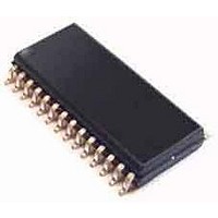
Page 46
... Package information 7 Package information In order to meet environmental requirements, ST offers these devices in different grades of ® ECOPACK packages, depending on their level of environmental compliance. ECOPACK specifications, grade definitions and product status are available at: www.st.com. ® ECOPACK trademark. Figure 30. SO-28 mechanical data and package dimensions DIM ...
Page 47
... Revision history Table 26. Document revision history Date 20-Oct-2003 13-Jan-2009 Revision 6 Initial release. Document reformatted. Document status changed from datasheet to “not for new design”. 7 Removed all refences to DIP28 package. Added Table 1: Device summary on page Updated Section 7: Package information on page Revision history Changes 1. ...
Page 48
... The ST logo is a registered trademark of STMicroelectronics. All other names are the property of their respective owners. Australia - Belgium - Brazil - Canada - China - Czech Republic - Finland - France - Germany - Hong Kong - India - Israel - Italy - Japan - Malaysia - Malta - Morocco - Singapore - Spain - Sweden - Switzerland - United Kingdom - United States of America ...