IRF7101PBF International Rectifier, IRF7101PBF Datasheet
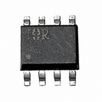
MOSFET N-CH 20V 3.5A 8-SOIC

IRF7101PBF

Manufacturer Part Number
IRF7101PBF
Description
MOSFET N-CH 20V 3.5A 8-SOIC
Manufacturer
International Rectifier
Series
HEXFET®r
Type
Power MOSFETr
Datasheets

Specifications of IRF7101PBF

Fet Type
2 N-Channel (Dual)
Fet Feature
Logic Level Gate
Rds On (max) @ Id, Vgs
100 mOhm @ 1.8A, 10V
Drain To Source Voltage (vdss)
20V
Current - Continuous Drain (id) @ 25° C
3.5A
Vgs(th) (max) @ Id
3V @ 250µA
Gate Charge (qg) @ Vgs
15nC @ 10V
Input Capacitance (ciss) @ Vds
320pF @ 15V
Power - Max
2W
Mounting Type
Surface Mount
Package / Case
8-SOIC (3.9mm Width)
Channel Type
N
Current, Drain
3.5 A
Package Type
SO-8
Polarization
N-Channel
Power Dissipation
2 W
Resistance, Drain To Source On
0.1 Ohm
Temperature, Operating, Maximum
+150 °C
Temperature, Operating, Minimum
-55 °C
Voltage, Breakdown, Drain To Source
20 V
Voltage, Gate To Source
±12 V
Number Of Elements
2
Polarity
N
Channel Mode
Enhancement
Drain-source On-res
0.1Ohm
Drain-source On-volt
20V
Gate-source Voltage (max)
±12V
Continuous Drain Current
3.5A
Operating Temp Range
-55C to 150C
Operating Temperature Classification
Military
Mounting
Surface Mount
Pin Count
8
Module Configuration
Dual
Transistor Polarity
N Channel
Continuous Drain Current Id
3.5A
Drain Source Voltage Vds
20V
On Resistance Rds(on)
100mohm
Rds(on) Test Voltage Vgs
10V
Rohs Compliant
Yes
Lead Free Status / RoHS Status
Lead free / RoHS Compliant

Available stocks

Company
Part Number
Manufacturer
Quantity
Price
Company:
Part Number:
IRF7101PBF
Quantity:
100
Thermal Resistance Ratings
Fourth Generation HEXFETs from International
Rectifier utilize advanced processing techniques to
achieve the lowest possible on-resistance per silicon
area. This benefit, combined with the fast switching
speed and ruggedized device design that HEXFET
Power MOSFETs are well known for, provides the
designer with an extremely efficient device for use in
a wide variety of applications.
The SO-8 has been modified through a customized
leadframe for enhanced thermal characteristics and
dual-die capability making it ideal in a variety of power
applications.
devices can be used in an application with dramatically
reduced board space. The package is designed for
vapor phase, infra red, or wave soldering techniques.
Power dissipation of greater than 0.8W is possible in
a typical PCB mount application.
Description
Absolute Maximum Ratings
I
I
I
P
V
dv/dt
T
D
D
DM
R
D
GS
J,
@ T
@ T
@T
T
Adavanced Process Technology
Ultra Low On-Resistance
Dual N-Channel MOSFET
Surface Mount
Available in Tape & Reel
Dynamic dv/dt Rating
Fast Switching
JA
STG
A
A
C
= 25°C
= 100°C
= 25°C
With these improvements, multiple
Maximum Junction-to-Ambient
Continuous Drain Current, V
Pulsed Drain Current
Power Dissipation
Linear Derating Factor
Gate-to-Source Voltage
Peak Diode Recovery dv/dt
Junction and Storage Temperature Range
Sodering Temperature, for 10 seconds
Parameter
Parameter
GS
GS
@ 10V
@ 10V
G 2
G 1
S 2
S 1
1
2
3
4
Top View
Min.
–––
300(1.6mm from case)
HEXFET
8
6
5
7
-55 to + 150
Max.
0.016
D1
D 1
D 2
D2
± 12
3.5
2.3
2.0
3.0
14
Typ.
S O -8
–––
®
IRF7101
R
Power MOSFET
DS(on)
V
I
DSS
D
PD - 9.871B
= 3.5A
Max
62.5
= 20V
= 0.10
°C/W
Units
Units
W/°C
V/nS
W
°C
A
V
8/25/97

Related parts for IRF7101PBF

IRF7101PBF Summary of contents

Page 1

Adavanced Process Technology Ultra Low On-Resistance Dual N-Channel MOSFET Surface Mount Available in Tape & Reel Dynamic dv/dt Rating Fast Switching Description Fourth Generation HEXFETs from International Rectifier utilize advanced processing techniques to achieve the lowest possible on-resistance per silicon ...

Page 2

IRF7101 Electrical Characteristics @ T Parameter V Drain-to-Source Breakdown Voltage (BR)DSS Breakdown Voltage Temp. Coefficient (BR)DSS J R Static Drain-to-Source On-Resistance DS(ON) V Gate Threshold Voltage GS(th) g Forward Transconductance fs I Drain-to-Source Leakage Current DSS Gate-to-Source ...

Page 3

IRF7101 ...

Page 4

IRF7101 ...

Page 5

D = 0.50 0.20 10 0.10 0.05 0.02 0.01 1 SINGLE PULSE (THERMAL RESPONSE) 0.1 0.0001 0.001 10 Fig 10. Maximum Effective Transient Thermal Impedance, Junction-to-Ambient 0.01 0 Rectangular Pulse Duration (sec) 1 IRF7101 ...

Page 6

IRF7101 10V Pulse Width µs Duty Factor Fig 11a. Switching Time Test Circuit Current Regulator Same Type as D.U.T. 50K .2 F 12V . 3mA I G Current Sampling Resistors Fig ...

Page 7

Peak Diode Recovery dv/dt Test Circuit + D.U Driver Gate Drive Period P.W. D.U.T. I Waveform SD Reverse Recovery Body Diode Forward Current D.U.T. V Waveform DS Re-Applied Voltage Body Diode Inductor Curent Ripple * ...

Page 8

IRF7101 Package Outline SO8 Outline 0.25 (.010 0.25 (.010) ...

Page 9

Tape & Reel Information SO8 Dimensions are shown in millimeters (inches TRO SIO ...

Related keywords