SI5904DC-T1-E3 Vishay, SI5904DC-T1-E3 Datasheet
SI5904DC-T1-E3
Specifications of SI5904DC-T1-E3
Available stocks


Related parts for SI5904DC-T1-E3


SI5904DC-T1-E3 Summary of contents
Page 1
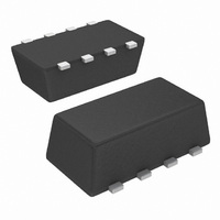
... Bottom View Ordering Information: Si5904DC-T1-E3 (Lead (Pb)-free) Si5904DC-T1-GE3 (Lead (Pb)-free and Halogen-free) ABSOLUTE MAXIMUM RATINGS T Parameter Drain-Source Voltage Gate-Source Voltage a Continuous Drain Current (T = 150 °C) J Pulsed Drain Current Continuous Source Current (Diode Conduction) a Maximum Power Dissipation Operating Junction and Storage Temperature Range ...
Page 2
... Si5904DC Vishay Siliconix SPECIFICATIONS °C, unless otherwise noted J Parameter Static Gate Threshold Voltage Gate-Body Leakage Zero Gate Voltage Drain Current a On-State Drain Current a Drain-Source On-State Resistance a Forward Transconductance a Diode Forward Voltage b Dynamic Total Gate Charge Gate-Source Charge Gate-Drain Charge Turn-On Delay Time ...
Page 3
... V - Source-to-Drain Voltage (V) SD Source-Drain Diode Forward Voltage Document Number: 71065 S10-0548-Rev. D, 08-Mar- 4 0.20 0.15 0. °C J 0.05 0.00 0.8 1.0 1.2 Si5904DC Vishay Siliconix 600 500 C iss 400 300 200 C oss 100 C rss Drain-to-Source Voltage (V) DS Capacitance ...
Page 4
... Si5904DC Vishay Siliconix TYPICAL CHARACTERISTICS 25 °C, unless otherwise noted 0.4 0 250 µA D 0.0 - 0.2 - 0 Temperature (°C) J Threshold Voltage 2 1 Duty Cycle = 0.5 0.2 0.1 0.1 0.05 0.02 Single Pulse 0. Duty Cycle = 0.5 0.2 0.1 0.1 0.05 0.02 Single Pulse 0.01 ...
Page 5
... E 1.825 1.90 1.975 0.072 E 1.55 1.65 1.70 0.061 1 e 0.65 BSC L 0.28 − 0.42 0.011 S 0.55 BSC 5_Nom Package Information Vishay Siliconix Backside View DETAIL X INCHES Nom Max − 0.043 0.012 0.014 0.006 0.008 − 0.0015 0.120 0.122 ...
Page 6
... The addition of a further copper area and/or the addition of vias to other board layers will enhance the performance still further. An example of this method is implemented on the Vishay 1 Siliconix Evaluation Board described in the next section ...
Page 7
... AN812 Vishay Siliconix Front of Board ChipFETr THERMAL PERFORMANCE Junction-to-Foot Thermal Resistance (the Package Performance) Thermal performance for the 1206-8 ChipFET measured as junction-to-foot thermal resistance is 30_C/W typical, 40_C/W maximum for the dual device. The “foot” is the drain lead of the device as it connects with the body. This is identical to the dual ...
Page 8
... Application Note 826 Vishay Siliconix RECOMMENDED MINIMUM PADS FOR 1206-8 ChipFET Return to Index Return to Index www.vishay.com 2 ® 0.093 (2.357) 0.026 0.016 (0.650) (0.406) Recommended Minimum Pads Dimensions in Inches/(mm) 0.010 (0.244) Document Number: 72593 Revision: 21-Jan-08 ...
Page 9
... Vishay product could result in personal injury or death. Customers using or selling Vishay products not expressly indicated for use in such applications their own risk and agree to fully indemnify and hold Vishay and its distributors harmless from and against any and all claims, liabilities, expenses and damages arising or resulting in connection with such use or sale, including attorneys fees, even if such claim alleges that Vishay or its distributor was negligent regarding the design or manufacture of the part ...