NSR0240V2T1G ON Semiconductor, NSR0240V2T1G Datasheet - Page 2
NSR0240V2T1G
Manufacturer Part Number
NSR0240V2T1G
Description
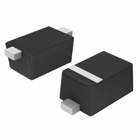
DIODE SCHOTTKY 40V 250MA SOD523
Manufacturer
ON Semiconductor
Datasheet
1.NSR0240V2T1G.pdf
(4 pages)
Specifications of NSR0240V2T1G
Voltage - Forward (vf) (max) @ If
700mV @ 200mA
Voltage - Dc Reverse (vr) (max)
40V
Current - Average Rectified (io)
250mA (DC)
Current - Reverse Leakage @ Vr
10µA @ 40V
Diode Type
Schottky
Speed
Fast Recovery =< 500ns, > 200mA (Io)
Reverse Recovery Time (trr)
3ns
Capacitance @ Vr, F
4pF @ 5V, 1MHz
Mounting Type
Surface Mount
Package / Case
SOD-523
Product
Schottky Diodes
Peak Reverse Voltage
40 V
Forward Continuous Current
0.25 A
Max Surge Current
1 A
Configuration
Single
Recovery Time
3 ns (Typ)
Forward Voltage Drop
0.7 V @ 0.2 A
Maximum Reverse Leakage Current
10 uA
Operating Temperature Range
- 55 C to + 150 C
Mounting Style
SMD/SMT
Lead Free Status / RoHS Status
Lead free / RoHS Compliant
Other names
NSR0240V2T1GOSTR
Available stocks
Company
Part Number
Manufacturer
Quantity
Price
Company:

Part Number:
NSR0240V2T1G
Manufacturer:
ON Semiconductor
Quantity:
9 400
Company:
Part Number:
NSR0240V2T1G
Manufacturer:
ON
Quantity:
30 000
Part Number:
NSR0240V2T1G
Manufacturer:
ON/安森美
Quantity:
20 000


1. Mounted onto a 4 in square FR−4 board 10 mm sq. 1 oz. Cu 0.06” thick single−sided. Operating to steady state.
2. Mounted onto a 4 in square FR−4 board 1 in sq. 1 oz. Cu 0.06” thick single−sided. Operating to steady state.
THERMAL CHARACTERISTICS
ELECTRICAL CHARACTERISTICS
Thermal Resistance
Junction−to−Ambient (Note 1)
Total Power Dissipation @ T
Thermal Resistance
Junction−to−Ambient (Note 2)
Total Power Dissipation @ T
Junction and Storage Temperature Range
Reverse Leakage
Forward Voltage
Total Capacitance
Reverse Recovery Time
Oscilloscope
50 W Output
50 W Input
Generator
(V
(V
(V
(I
(I
(I
(V
(I
F
F
F
F
Pulse
R
R
R
R
= 10 mA)
= 100 mA)
= 200 mA)
= I
= 10 V)
= 25 V)
= 40 V)
= 5.0 V, f = 1 MHz)
R
= 10 mA, I
Adjust for I
+
R
DC Current
L
750 mH
Source
= 50 W
0.1 mF
R
RM
1. DC Current Source is adjusted for a Forward Current (I
2. Pulse Generator Output is adjusted for a Peak Reverse Recovery Current I
3. Pulse Generator transition time << t
4. I
5. t
= 1.0 mA)
Characteristic
R(REC)
p
» t
A
A
Characteristic
−
= 25°C
= 25°C
rr
I
is measured at 1 mA. Typically 0.1 X I
DUT
Current
Transformer
F
0.1 mF
Figure 1. Recovery Time Equivalent Test Circuit
(T
A
= 25°C unless otherwise noted)
http://onsemi.com
rr
.
2
RM
Symbol
or 0.25 X I
T
R
R
J
Symbol
P
P
, T
qJA
qJA
D
D
V
CT
I
t
stg
R
rr
F
F
) of 10 mA.
I
RM
0 V
I
V
F
RM
R
.
(I
F
Min
= I
t
r
Pulse Generator
at i
RM
−55 to +150
Output Pulse
R(REC)
10%
90%
= 10 mA; measured
Output
RM
Max
600
200
300
400
t
p
t
rr
i
R(REC)
of 10 mA.
= 1 mA)
Typ
345
485
580
0.2
0.5
4.0
3.0
= 1 mA
0.55
Max
390
550
700
2.0
10
°C/W
°C/W
Unit
mW
mW
°C
Unit
mV
mA
pF
ns
Related parts for NSR0240V2T1G
Image
Part Number
Description
Manufacturer
Datasheet
Request
R

Part Number:
Description:
ON Semiconductor [VOLTAGE REGULATOR]
Manufacturer:
ON Semiconductor
Datasheet:
Part Number:
Description:
357-036-542-201 CARDEDGE 36POS DL .156 BLK LOPRO
Manufacturer:
ON Semiconductor
Datasheet:
Part Number:
Description:
357-036-542-201 CARDEDGE 36POS DL .156 BLK LOPRO
Manufacturer:
ON Semiconductor
Datasheet:
Part Number:
Description:
357-036-542-201 CARDEDGE 36POS DL .156 BLK LOPRO
Manufacturer:
ON Semiconductor
Datasheet:
Part Number:
Description:
357-036-542-201 CARDEDGE 36POS DL .156 BLK LOPRO
Manufacturer:
ON Semiconductor
Datasheet:
Part Number:
Description:
357-036-542-201 CARDEDGE 36POS DL .156 BLK LOPRO
Manufacturer:
ON Semiconductor
Datasheet:
Part Number:
Description:
357-036-542-201 CARDEDGE 36POS DL .156 BLK LOPRO
Manufacturer:
ON Semiconductor
Datasheet:
Part Number:
Description:
357-036-542-201 CARDEDGE 36POS DL .156 BLK LOPRO
Manufacturer:
ON Semiconductor
Datasheet:
Part Number:
Description:
357-036-542-201 CARDEDGE 36POS DL .156 BLK LOPRO
Manufacturer:
ON Semiconductor
Datasheet:
Part Number:
Description:
357-036-542-201 CARDEDGE 36POS DL .156 BLK LOPRO
Manufacturer:
ON Semiconductor
Datasheet:
Part Number:
Description:
357-036-542-201 CARDEDGE 36POS DL .156 BLK LOPRO
Manufacturer:
ON Semiconductor
Datasheet:
Part Number:
Description:
Manufacturer:
ON Semiconductor
Datasheet:
Part Number:
Description:
Manufacturer:
ON Semiconductor
Datasheet:
Part Number:
Description:
Manufacturer:
ON Semiconductor
Datasheet: