V60100C-E3/45 Vishay, V60100C-E3/45 Datasheet

DIODE SCHOTTKY 100V 30A TO-220AB

V60100C-E3/45

Manufacturer Part Number
V60100C-E3/45
Description
DIODE SCHOTTKY 100V 30A TO-220AB
Manufacturer
Vishay
Datasheet

Specifications of V60100C-E3/45

Voltage - Forward (vf) (max) @ If
790mV @ 30A
Current - Reverse Leakage @ Vr
1mA @ 100V
Current - Average Rectified (io) (per Diode)
30A
Voltage - Dc Reverse (vr) (max)
100V
Diode Type
Schottky
Speed
Fast Recovery =< 500ns, > 200mA (Io)
Diode Configuration
1 Pair Common Cathode
Mounting Type
Through Hole
Package / Case
TO-220-3 (Straight Leads)
Product
Schottky Rectifiers
Peak Reverse Voltage
100 V
Forward Continuous Current
60 A
Max Surge Current
320 A
Configuration
Dual Common Cathode
Forward Voltage Drop
0.79 V at 30 A
Maximum Reverse Leakage Current
1000 uA
Operating Temperature Range
- 40 C to + 150 C
Mounting Style
Through Hole
Lead Free Status / RoHS Status
Lead free / RoHS Compliant
Reverse Recovery Time (trr)
-
Lead Free Status / RoHS Status
Lead free / RoHS Compliant, Lead free / RoHS Compliant
Other names
V60100C-E3/45GI
Document Number: 88942
Revision: 24-Jun-09
PRIMARY CHARACTERISTICS
MAXIMUM RATINGS (T
PARAMETER
Maximum repetitive peak reverse voltage
Maximum average forward rectified current (fig. 1)
Peak forward surge current 8.3 ms single half
sine-wave superimposed on rated load per diode
Non-repetitive avalanche energy
at T
Peak repetitive reverse current at t
T
Voltage rate of change (rated V
Operating junction and storage temperature range
J
= 38 °C ± 2 °C per diode
J
= 25 °C, L = 140 mH per diode
V
Dual High-Voltage Trench MOS Barrier Schottky Rectifier
PIN 1
PIN 3
F
at I
T
TO-220AB
V
I
V60100C
J
I
F(AV)
FSM
RRM
F
max.
= 30 A
PIN 2
CASE
1
2
PDD-Americas@vishay.com, PDD-Asia@vishay.com,
TMBS
3
For technical questions within your region, please contact one of the following:
R
)
p
A
= 2 µs, 1 kHz,
= 25 °C unless otherwise noted)
®
PIN 2
PIN 1
2 x 30 A
Ultra Low V
150 °C
0.66 V
100 V
320 A
K
VB60100C
TO-263AB
per device
per diode
HEATSINK
1
K
New Product
2
F
= 0.36 V at I
SYMBOL
T
J
V
I
dV/dt
I
I
F(AV)
, T
E
RRM
FSM
RRM
AS
STG
FEATURES
TYPICAL APPLICATIONS
For use in high frequency converters, switching power
supplies, freewheeling diodes, OR-ing diode, dc-to-dc
converters and reverse battery protection.
MECHANICAL DATA
Case: TO-220AB and TO-263AB
Molding compound meets UL 94 V-0 flammability
rating
Base P/N-E3 - RoHS compliant, commercial grade
Terminals: Matte tin plated leads, solderable per
J-STD-002 and JESD 22-B102
E3 suffix meets JESD 201 class 1A whisker test
Polarity: As marked
Mounting Torque: 10 in-lbs maximum
• Trench MOS Schottky technology
• Low forward voltage drop, low power
• High efficiency operation
• Low thermal resistance
• Meets MSL level 1, per J-STD-020, LF maximum
• Solder bath temperature 275 °C maximum, 10 s,
• Compliant to RoHS directive 2002/95/EC and in
losses
peak of 245 °C (for TO-263AB package)
per JESD 22-B106 (for TO-220AB)
accordance to WEEE 2002/96/EC
F
PDD-Europe@vishay.com
= 5 A
Vishay General Semiconductor
V60100C
V60100C & VB60100C
- 40 to + 150
10 000
100
320
450
1.0
60
30
VB60100C
www.vishay.com
UNIT
V/µs
mJ
°C
V
A
A
A
1

Related parts for V60100C-E3/45

V60100C-E3/45 Summary of contents

Page 1

... E3 suffix meets JESD 201 class 1A whisker test Polarity: As marked Mounting Torque: 10 in-lbs maximum SYMBOL V RRM per device I F(AV) per diode I FSM RRM dV/ STG PDD-Europe@vishay.com V60100C & VB60100C Vishay General Semiconductor = 5 A V60100C VB60100C 100 60 30 320 450 1.0 10 000 - 150 www.vishay.com UNIT V/µs °C ...

Page 2

... V60100C & VB60100C Vishay General Semiconductor ELECTRICAL CHARACTERISTICS (T PARAMETER Breakdown voltage (1) Instantaneous forward voltage per diode (2) Reverse current at rated V per diode R Notes (1) Pulse test: 300 µs pulse width duty cycle (2) Pulse test: Pulse width ≤ THERMAL CHARACTERISTICS (T PARAMETER Typical thermal resistance per diode ...

Page 3

... Vishay General Semiconductor 10 000 1000 100 0.8 1 0.1 Figure 5. Typical Junction Capacitance Per Diode 100 0.01 Figure 6. Typical Transient Thermal Impedance Per Diode PDD-Europe@vishay.com V60100C & VB60100C ° 1.0 MHz mVp-p sig 1 10 100 Reverse Voltage (V) 0 100 t - Pulse Duration (s) www ...

Page 4

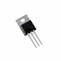
... V60100C & VB60100C Vishay General Semiconductor PACKAGE OUTLINE DIMENSIONS in inches (millimeters) 0.160 (4.06) 0.140 (3.56) 0.057 (1.45) 0.045 (1.14) 0.105 (2.67) 0.095 (2.41) 0.104 (2.65) 0.096 (2.45) 0.411 (10.45) 0.380 (9.65) 0.245 (6.22) MIN. K 0.360 (9.14) 0.320 (8.13) 0.624 (15.85 0.591 (15.00) ...

Page 5

... Vishay product could result in personal injury or death. Customers using or selling Vishay products not expressly indicated for use in such applications their own risk and agree to fully indemnify and hold Vishay and its distributors harmless from and against any and all claims, liabilities, expenses and damages arising or resulting in connection with such use or sale, including attorneys fees, even if such claim alleges that Vishay or its distributor was negligent regarding the design or manufacture of the part ...

Related keywords