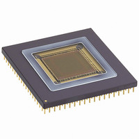
MT9M413C36STM Aptina LLC, MT9M413C36STM Datasheet
MT9M413C36STM
Specifications of MT9M413C36STM


Related parts for MT9M413C36STM


MT9M413C36STM Summary of contents
Page 1
CMOS ACTIVE-PIXEL DIGITAL IMAGE SENSOR Description The MI-MV13 is a 1,280H x 1,024V (1.3 megapixel) CMOS digital image sensor capable of 500 frames-per- second (fps) operation. Its TrueSNAP™ electronic shutter allows simultaneous exposure of the entire pixel array. Available ...
Page 2
General The MI-MV13 is a 1280H x 1024V (1.31 megapixel) CMOS digital image sensor capable of 500 frames-per- second (fps) operation. Its TrueSNAP™ electronic shutter allows simultaneous exposure of the entire pixel array. Available in color or monochrome, the sen- ...
Page 3
Figure 2: Sensor Architecture (not to scale) DIGITAL CONTROL Pixel TX_N Photo Detector Memory PG_N VRST_PIX 09005aef806807ca MT9M413C36STC.fm - Ver. 3.0 1/04 EN 1.3-MEGAPIXEL CMOS ACTIVE-PIXEL SENSE AMPS MEMORY TOP ADCs PIXEL ARRAY BOTTOM ADCs Figure 3: Signal Path Diagram ...
Page 4
TX_N PG_N ROW 10 LogicRST Row Timing RowSTRT Block RowDone SRAM Data Shift / Read Read Control 09005aef806807ca MT9M413C36STC.fm - Ver. 3.0 1/04 EN 1.3-MEGAPIXEL CMOS ACTIVE-PIXEL Figure 4: Functional Block Diagram PIXEL ARRAY ADC #1 Sample Shift 1280 x ...
Page 5
External Control Sequence The MI-MV13 includes on-chip timing and control circuitry to control most of the pixel, ADC, and output multiplexing operations. However, the sensor still requires a controller (FPGA, CPLD, ASIC, etc.) to guide it through the full sequence ...
Page 6
Figure 5: Example 1 - Row 4 of the MI-MV13 Being Digitized Controller Controller ROW_ADDR ROW_ADDR ROW_STRT_N ROW_STRT_N LD_SHFT_N SYSCLK ...
Page 7
LD_SHFT_N This signal transfers the digitized data from the ADC register to the output register (1280 x 10-bit) and gates the power to the sense amplifiers. The first data (col- umns 1-10) are available for output at the third rising ...
Page 8
ROW_ADDR [0:9] ROW_STRT_N ROW_DONE_N LD_ SHFT_N DATA_READ_EN_N DATA [0:99] ROW1023 PG_N=PG1+PG2 TX_ N The MI-MV13 contains special self-calibrating cir- cuitry that enables it to reduce its own column-wise fixed-pattern noise. This calibration process consists of connecting a calibration ...
Page 9
Figure 8: Typical I/O Signal Timing (Initialization Sequence) CAL_STRT_N CAL_DONE_N SYSCLK LRST_N CAL_DONE_N SYSCLK CAL_STRT_N CAL_STRT_N is a two-clock cycle-wide active-low pulse that initiates the ADC calibration sequence. The pulse must not be actuated for 1 microsecond after either power-up ...
Page 10
Electronic Shutter The MI-MV13 is intended to be operated primarily with the TrueSNAP freeze-frame electronic shutter, but is also capable of operating in Electronic Rolling Shut- ter (ERS) mode. With TrueSNAP the shutter can be operated to generate continuous video ...
Page 11
Figure 10: Typical Example of TrueSNAP Sequential Mode: Exposure Following Readout PG_N TX_N ROW_ADDR 1023 Exposure Exposure time time Readout 0 TrueSNAP Single Frame The MI-MV13 can run in single frame or snap-shot mode in which one image is captured. ...
Page 12
Table 3: Pin Description (Continued) PIN NUMBER(S) SIGNAL NAME T15 DATA5 U16 DATA6 R14 DATA7 V18 DATA8 P15 DATA9 D14 DATA10 A16 DATA11 C16 DATA12 E13 DATA13 D15 DATA14 A18 DATA15 E14 DATA16 B18 DATA17 D17 DATA18 E16 DATA19 W11 ...
Page 13
Table 3: Pin Description (Continued) PIN NUMBER(S) SIGNAL NAME C8 DATA50 A7 DATA51 D9 DATA52 E9 DATA53 A8 DATA54 C10 DATA55 A9 DATA56 D10 DATA57 B10 DATA58 C11 DATA59 T4 DATA60 R6 DATA61 V3 DATA62 W3 DATA63 R7 DATA64 W4 ...
Page 14
Table 3: Pin Description (Continued) PIN NUMBER(S) SIGNAL NAME E4 DATA95 C2 DATA96 A1 DATA97 F5 DATA98 B2 DATA99 L3 CAL_DONE_N L2 CAL_STRT_N F1 DARK_OFF_EN_N J4, N15, J16 VDD H3, H18, T18 DGND K2 LD_SHFT_N J3 DATA_READ_EN_N L1 LRST_N ROW_ADDR ...
Page 15
Table 3: Pin Description (Continued) PIN NUMBER(S) SIGNAL NAME G16, E10, C13, B4, VDD_IO B8, C7, F4, M2, B14, F15, R13, T12, B1, H4, N4, R3, T5, U5, W7, U9, U11, T16, B16 G5, D4, G4, K3, DGND_IO N5, P5, ...
Page 16
Table 3: Pin Description (Continued) PIN NUMBER(S) SIGNAL NAME R16 VLP_DRV L4 TX_N M3 PG_N L18, P16, J17 VRST_PIX L16 VREF4 E5,C3,C1, D2, E1,F2, F3, G1, H1, J2, J1, K1, M1, N1, N2, P1,R1, R2, T3, U2, R5, U3, V2, ...
Page 17
G18 _____ H16 _____ H15 _____ F18 _____ G17 _____ F17 _____ E18 _____ G15 _____ F16 _____ D18 _____ G3 _____ J3 _____ K2 Controller ________ L3 _____ L5 Interface ________ L2 _____ K4 ________ F1 _____ H2 ...
Page 18
Electrical Specifications Table 4: AC Electrical Characteristics (Vsupply = 3.3V ± 0.3V) SYMBOL CHARACTERISTIC Tplh Data output propagation delay for low to high trans. Tphl Data output propagation delay for high to low trans. Tsetup Setup time for input to ...
Page 19
Table 6: Absolute Maximum Ratings SYMBOL PARAMETER Vpwr DC Supply Voltage Vin DC Input Voltage Vout DC Output Voltage I DC Current Drain per Pin (Any I/ Current Drain, Vpwr and Vgnd NOTE: Vpwr = VDD = VAA ...
Page 20
Analog Voltage Setting Considerations The values suggested in the Typical Values column in the “AC Electrical Characteristics” on page 18 should be the starting point for setting the analog voltages. Additionally useful to refer to the “Signal Path ...
Page 21
Figure 16: Bayer Pattern (Pixel Color Pattern Detail) 09005aef806807ca MT9M413C36STC.fm - Ver. 3.0 1/04 EN 1.3-MEGAPIXEL CMOS ACTIVE-PIXEL Figure 15: Pixel Array Layout Megapixel (1280H x 1024V) 1280 x 1024 active pixels (0,0) ...
Page 22
Optical Specification Table 9: Image Sensor Characteristics T = 25°C A SYMBOL PARAMETER R Responsivity (ADC VREF=1V) I Nsat Pixel saturation level NADC DC noise + DNL 1 Dark signal non-uniformity, high spatial frequency DSNU Dark signal non-uniformity, ...
Page 23
Green 1 pixels 400 09005aef806807ca MT9M413C36STC.fm - Ver. 3.0 1/04 EN 1.3-MEGAPIXEL CMOS ACTIVE-PIXEL Figure 17: Quantum Efficiency Quantum Effficiency for Color 500 600 700 800 ...
Page 24
Lens Selection Much of the specific information in this section is explained in detail at http://www.micron.com/prod- ucts/imaging/technology/index.html on our web site. The following information applies specifically to the MI-MV13 megapixel image sensor. Format The diagonal of the image sensor array, ...
Page 25
MTF ranges from zero (no information gets through) to 100 (all information gets through), and is always specified in terms of informa- tion density. In most ...
Page 26
Figure 18: C-Mount Lens Shroud for MI-MV13 and Socket BASE 2.50” 0.125 0.125 0.25” LID 2.50” 1.25 0.125” 0.0 0.0 NOTE: This shroud is designed to accommodate the MI-MV13 when it is inserted into a PGA socket. These dimensions are ...
Page 27
Figure 19: 280-Pin Ceramic PGA Package INDEX 0.003 (0, 0) Notes: 1. Sensor is centered on package, pixel array is off-center. ± 2. Die offset is 10 mils in both the X and Y directions. ± 3. Die rotation is ...
Page 28
Figure 20: 280-Pin Ceramic PGA Package UNITS: INCHES Notes: 1. Die thickness 28.5 mils ± 1 mil. 2. Die epoxy thickness 1 mil. 3. D-263 glass lid thickness 31 ± 2 mils. 4. Glass lid epoxy thickness 1 mil. 09005aef806807ca ...
Page 29
Figure 21: 280-Pin Ceramic PGA Package 0.100 typ 09005aef806807ca MT9M413C36STC.fm - Ver. 3.0 1/04 EN 1.3-MEGAPIXEL CMOS ACTIVE-PIXEL Bottom View 1.800± 0.012 (P = 0.100 X 18) (281X) 067 TYP. DIA. EXTRA PIN ...
Page 30
Environmental Table 13: Absolute Maximum Ratings SYMBOL PARAMETER T Storage Temperature Range storage T Lead Temperature (10 second soldering) lead Document History Table 14: Document Change History CHANGED CHANGE DATE BY Ver. 3.0 Ver. 3.0 1/7/04 EJakl 8000 S. Federal ...