SA606DK,118 NXP Semiconductors, SA606DK,118 Datasheet - Page 23
SA606DK,118
Manufacturer Part Number
SA606DK,118
Description
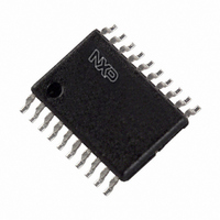
IC MIXER FM IF SYSTEM LP 20-SSOP
Manufacturer
NXP Semiconductors
Series
SA606r
Datasheet
1.SA606DK01118.pdf
(29 pages)
Specifications of SA606DK,118
Rf Type
Cellular, ASK, FSK
Frequency
150MHz
Number Of Mixers
2
Gain
17dB
Noise Figure
6.2dB
Secondary Attributes
Up Converter
Current - Supply
4.2mA
Voltage - Supply
2.7 V ~ 7 V
Package / Case
20-LSSOP (0.173", 4.4mm)
Lead Free Status / RoHS Status
Lead free / RoHS Compliant
Other names
568-1102-2
935051650118
SA606DK-T
935051650118
SA606DK-T


NXP Semiconductors
16. Soldering of SMD packages
SA606
Product data sheet
16.1 Introduction to soldering
16.2 Wave and reflow soldering
16.3 Wave soldering
This text provides a very brief insight into a complex technology. A more in-depth account
of soldering ICs can be found in Application Note AN10365 “Surface mount reflow
soldering description”.
Soldering is one of the most common methods through which packages are attached to
Printed Circuit Boards (PCBs), to form electrical circuits. The soldered joint provides both
the mechanical and the electrical connection. There is no single soldering method that is
ideal for all IC packages. Wave soldering is often preferred when through-hole and
Surface Mount Devices (SMDs) are mixed on one printed wiring board; however, it is not
suitable for fine pitch SMDs. Reflow soldering is ideal for the small pitches and high
densities that come with increased miniaturization.
Wave soldering is a joining technology in which the joints are made by solder coming from
a standing wave of liquid solder. The wave soldering process is suitable for the following:
Not all SMDs can be wave soldered. Packages with solder balls, and some leadless
packages which have solder lands underneath the body, cannot be wave soldered. Also,
leaded SMDs with leads having a pitch smaller than ~0.6 mm cannot be wave soldered,
due to an increased probability of bridging.
The reflow soldering process involves applying solder paste to a board, followed by
component placement and exposure to a temperature profile. Leaded packages,
packages with solder balls, and leadless packages are all reflow solderable.
Key characteristics in both wave and reflow soldering are:
Key characteristics in wave soldering are:
•
•
•
•
•
•
•
•
•
•
Through-hole components
Leaded or leadless SMDs, which are glued to the surface of the printed circuit board
Board specifications, including the board finish, solder masks and vias
Package footprints, including solder thieves and orientation
The moisture sensitivity level of the packages
Package placement
Inspection and repair
Lead-free soldering versus SnPb soldering
Process issues, such as application of adhesive and flux, clinching of leads, board
transport, the solder wave parameters, and the time during which components are
exposed to the wave
Solder bath specifications, including temperature and impurities
All information provided in this document is subject to legal disclaimers.
Rev. 4 — 12 April 2011
Low-voltage high performance mixer FM IF system
© NXP B.V. 2011. All rights reserved.
SA606
23 of 29
Related parts for SA606DK,118
Image
Part Number
Description
Manufacturer
Datasheet
Request
R

Part Number:
Description:
IC MIXER FM IF SYSTEM LV 20-SSOP
Manufacturer:
NXP Semiconductors
Datasheet:

Part Number:
Description:
Manufacturer:
NXP Semiconductors
Datasheet:

Part Number:
Description:
Up-Down Converters LV NB FM IF RCVR SYS
Manufacturer:
NXP Semiconductors
Datasheet:

Part Number:
Description:
IC MIXER FM IF SYSTEM LP 20-SSOP
Manufacturer:
NXP Semiconductors
Datasheet:
Part Number:
Description:
IC MIXER FM IF SYSTEM LP 20-SSOP
Manufacturer:
NXP Semiconductors
Datasheet:

Part Number:
Description:
Up-Down Converters LV NB FM IF RCVR SYS
Manufacturer:
NXP Semiconductors
Datasheet:

Part Number:
Description:
IC MIXER FM IF SYSTEM LV SOT163
Manufacturer:
NXP Semiconductors
Datasheet:
Part Number:
Description:
IC MIXER FM IF SYSTEM LP 20-SOIC
Manufacturer:
NXP Semiconductors
Datasheet:
Part Number:
Description:
Up-Down Converters LV HI PERF MIXER FM IF SYSTEM
Manufacturer:
NXP Semiconductors
Datasheet:

Part Number:
Description:
IC DVR HBRIDGE 80V 15A 12-PWRSIP
Manufacturer:
Cirrus Logic Inc
Datasheet:

Part Number:
Description:
TRANSIENT SUPPRESSOR DIODE,SINGLE,UNIDIRECTIONAL,60V V(RWM),DO-15
Manufacturer:
Vishay
Datasheet:

Part Number:
Description:
TVS Diodes - Transient Voltage Suppressors 500W 60V 10% Unidir
Manufacturer:
Vishay Semiconductors
Datasheet:
Part Number:
Description:
TVS Diodes - Transient Voltage Suppressors 500W 60V Unidirect
Manufacturer:
Vishay Semiconductors
Datasheet:
Part Number:
Description:
TVS Diodes - Transient Voltage Suppressors 500W 60V 10% Unidir
Manufacturer:
Vishay Semiconductors
Datasheet: