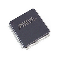
EPM1270GT144I5N Altera, EPM1270GT144I5N Datasheet - Page 35

EPM1270GT144I5N
Manufacturer Part Number
EPM1270GT144I5N
Description
MAX II
Manufacturer
Altera
Datasheet
1.EPM1270GT144I5N.pdf
(88 pages)
Specifications of EPM1270GT144I5N
Family Name
MAX II
Memory Type
Flash
# Macrocells
980
Frequency (max)
1.8797GHz
Propagation Delay Time
10ns
Number Of Logic Blocks/elements
127
# I/os (max)
116
Operating Supply Voltage (typ)
1.8V
In System Programmable
Yes
Operating Supply Voltage (min)
1.71V
Operating Supply Voltage (max)
1.89V
Operating Temp Range
-40C to 100C
Operating Temperature Classification
Industrial
Mounting
Surface Mount
Pin Count
144
Package Type
TQFP
Lead Free Status / Rohs Status
Compliant
Available stocks
Company
Part Number
Manufacturer
Quantity
Price
Company:
Part Number:
EPM1270GT144I5N
Manufacturer:
ALTERA
Quantity:
612
Chapter 2: MAX II Architecture
I/O Structure
Figure 2–22. MAX II I/O Banks for EPM240 and EPM570
Notes to
(1)
(2)
© October 2008 Altera Corporation
Figure 2–22
Figure 2–22
Figure
2–22:
is a top view of the silicon die.
is a graphical representation only. Refer to the pin list and the Quartus II software for exact pin locations.
I/O Bank 1
Table 2–4
Table 2–4. MAX II I/O Standards
The EPM240 and EPM570 devices support two I/O banks, as shown in
Each of these banks support all the LVTTL and LVCMOS standards shown in
Table
The EPM1270 and EPM2210 devices support four I/O banks, as shown in
Each of these banks support all of the LVTTL and LVCMOS standards shown in
Table
clamping diode on inputs and PCI drive compliance on outputs. You must use Bank 3
for designs requiring PCI compliant I/O pins. The Quartus II software automatically
places I/O pins in this bank if assigned with the PCI I/O standard.
3.3-V LVTTL/LVCMOS
2.5-V LVTTL/LVCMOS
1.8-V LVTTL/LVCMOS
1.5-V LVCMOS
3.3-V PCI
Note to
(1) The 3.3-V PCI compliant I/O is supported in Bank 3 of the EPM1270 and EPM2210
devices.
I/O Standard
2–4. PCI compliant I/O is not supported in these devices and banks.
2–4. PCI compliant I/O is supported in Bank 3. Bank 3 supports the PCI
Table
(1)
describes the I/O standards supported by MAX II devices.
2–4:
All I/O Banks Support
■
■
■
■
3.3-V LVTTL/LVCMOS
2.5-V LVTTL/LVCMOS
1.8-V LVTTL/LVCMOS
1.5-V LVCMOS
Single-ended
Single-ended
Single-ended
Single-ended
Single-ended
(Note
Type
1),
(2)
Output Supply Voltage
(VCCIO) (V)
3.3
2.5
1.8
1.5
3.3
I/O Bank 2
MAX II Device Handbook
Figure
Figure
2–22.
2–23.
2–27


