CY7C168A-20PXC Cypress Semiconductor Corp, CY7C168A-20PXC Datasheet
CY7C168A-20PXC
Specifications of CY7C168A-20PXC
Available stocks


Related parts for CY7C168A-20PXC

CY7C168A-20PXC Summary of contents
Page 1
... Cypress Semiconductor Corporation Document Number: 38-05029 Rev. *C Functional Description The CY7C168A is a high-performance CMOS static RAM organized as 4096 by 4-bits. Easy memory expansion is provided by an active LOW chip enable (CE) and three-state drivers. The CY7C168A has an automatic power-down feature, reducing the power consumption by 77% when deselected. ...
Page 2
... Switching Characteristics ................................................ 6 Switching Waveforms ...................................................... 6 Typical DC and AC Characteristics ................................ 8 Document Number: 38-05029 Rev. *C Ordering Information ........................................................ 9 Ordering Code Definitions ........................................... 9 Package Diagram .............................................................. 9 Acronyms ........................................................................ 10 Document Conventions ................................................. 10 Units of Measure ....................................................... 10 Document History Page ................................................. 11 Sales, Solutions, and Legal Information ...................... 12 Worldwide Sales and Design Support ....................... 12 Products .................................................................... 12 PSoC Solutions ......................................................... 12 CY7C168A Page [+] Feedback ...
Page 3
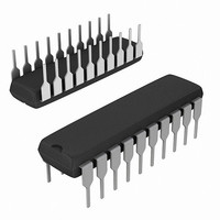
... Pin Configuration Selection Guide Maximum access time (ns) Maximum operating current (mA) Document Number: 38-05029 Rev. *C Figure 1. DIP Top View 7C168A GND C168A-2 Commercial Military CY7C168A 7C168A- 100 Page [+] Feedback ...
Page 4
... V = Min 8 GND < V < GND < V < output disabled Max GND CC OUT V = Max OUT Max > 0.3 V Max > CY7C168A Ambient Temperature V CC 10 +70 C 7C168A-20 Min Max Unit 2.4 – V – 0 0.5 0.8 V 10 +10 µA 10 +10 µA 350 – ...
Page 5
... Tested initially and after any design or process changes that may affect these parameters. Document Number: 38-05029 Rev. *C Test Conditions = 25 MHz 481 3 GND 255 < JIG AND (b) SCOPE C168A-3 1.73 V CY7C168A Max Unit = 5 ALL INPUT PULSES 90% 90% 10% 10% < C168A-4 Page [+] Feedback ...
Page 6
... WE is HIGH for read cycle. 9. Device is continuously selected Document Number: 38-05029 Rev. *C Description [8, 9] Figure 2. Read Cycle No for all devices. Transition is measured 500 mV from steady state voltage with specified loading in part (b) is less than CY7C168A 7C168A-20 Unit Min. Max. 20 – ns – – ns – 20 ...
Page 7
... DATA VALID Figure 4. Write Cycle No.1 (WE Controlled SCE PWE t SD DATA VALID IN t HZWE HIGH IMPEDANCE Figure 5. Write Cycle No. 2 (CS Controlled SCE PWE t SD DATA VALID IN t HZWE CY7C168A t HZCE HIGH IMPEDANCE 50 RCH C168A-6 [12 LZWE C168A-7 [12, 13 HIGH IMPEDANCE C168A-8 Page [+] Feedback ...
Page 8
... AMBIENT TEMPERATURE (°C) TYPICAL ACCESS TIME CHANGE vs. OUTPUT LOADING 30.0 25.0 20.0 15 25°C A 5.0 0.0 0 200 400 600 800 1000 CAPACITANCE (pF) CY7C168A OUTPUT SOURCE CURRENT vs. OUTPUT VOLTAGE 120 100 5. 25° 0.0 1.0 2.0 3.0 4.0 OUTPUT VOLTAGE (V) OUTPUT SINK CURRENT vs ...
Page 9
... Ordering Information Speed (ns) Ordering Code 20 CY7C168A-20PXC Ordering Code Definitions 168A - Temperature range (Commercial 20-lead molded DIP (Pb-free Speed grade 168A = 4 K × 4 architecture Family Fast asynchronous SRAM Company ID Cypress Package Diagram Document Number: 38-05029 Rev. *C Package Package Type Name P5 20-Lead Molded DIP Figure 6 ...
Page 10
... TTL transistor-transistor logic WE write enable Document Number: 38-05029 Rev. *C Document Conventions Units of Measure Symbol Unit of Measure ns nano seconds V Volts µA micro Amperes mA milli Amperes mV milli Volts mW milli Watts pF pico Farad °C degree Celcius W Watts % percent CY7C168A Page [+] Feedback ...
Page 11
... Updated Operating Range section with only Commercial temperature range Updated Electrical Characteristics section with only 7C168A-20 values Updated Switching Characteristics section with only 7C168A-20 values Updated Ordering Information section with only CY7C168A-20PXC Ordering Code Updated Package Diagram with only the latest revision of “20-Lead (300-Mil) Molded DIP P5” ...
Page 12
... Cypress against all charges. Use may be limited by and subject to the applicable Cypress software license agreement. Document Number: 38-05029 Rev. *C All products and company names mentioned in this document may be the trademarks of their respective holders. cypress.com/go/plc Revised November 30, 2010 CY7C168A PSoC Solutions psoc.cypress.com/solutions PSoC 1 | PSoC 3 ...