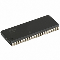
CY7C1041D-10VXIT Cypress Semiconductor Corp, CY7C1041D-10VXIT Datasheet - Page 3

CY7C1041D-10VXIT
Manufacturer Part Number
CY7C1041D-10VXIT
Description
CY7C1041D-10VXIT
Manufacturer
Cypress Semiconductor Corp
Datasheet
1.CY7C1041D-10ZSXI.pdf
(11 pages)
Specifications of CY7C1041D-10VXIT
Format - Memory
RAM
Memory Type
SRAM - Asynchronous
Memory Size
4M (256K x 16)
Speed
10ns
Interface
Parallel
Voltage - Supply
4.5 V ~ 5.5 V
Operating Temperature
-40°C ~ 85°C
Package / Case
44-SOJ
Lead Free Status / RoHS Status
Lead free / RoHS Compliant
Document #: 38-05472 Rev. *E
Thermal Resistance
AC Test Loads and Waveforms
Switching Characteristics
Read Cycle
t
t
t
t
t
t
t
t
t
t
t
t
t
t
t
Notes:
power
RC
AA
OHA
ACE
DOE
LZOE
HZOE
LZCE
HZCE
PU
PD
DBE
LZBE
HZBE
5. AC characteristics (except High-Z) are tested using the load conditions shown in Figure (a). High-Z characteristics are tested for all speeds using the test load
6. Test conditions assume signal transition time of 3 ns or less, timing reference levels of 1.5V, input pulse levels of 0 to 3.0V, and output loading of the specified
7. t
8. t
9. At any given temperature and voltage condition, t
Parameter
shown in Figure (c)
I
Parameter
OL
POWER
HZOE
* CAPACITIVE LOAD CONSISTS
OF ALL COMPONENTS OF THE
TEST ENVIRONMENT
/I
OH
10 ns device
JA
JC
, t
HZCE
and 30-pF load capacitance.
gives the minimum amount of time that the power supply should be at typical V
, t
OUTPUT
HZBE
Thermal Resistance
(Junction to Ambient)
Thermal Resistance
(Junction to Case)
, and t
OUTPUT
V
Read Cycle Time
Address to Data Valid
Data Hold from Address Change
CE LOW to Data Valid
OE LOW to Data Valid
OE LOW to Low Z
OE HIGH to High Z
CE LOW to Low Z
CE HIGH to High Z
CE LOW to Power-Up
CE HIGH to Power-Down
Byte Enable to Data Valid
Byte Enable to Low Z
Byte Disable to High Z
High-Z Characteristics:
CC
HZWE
INCLUDING
JIG AND
SCOPE
(typical) to the First Access
Description
5V
are specified with a load capacitance of 5 pF as in part (c) of AC Test Loads. Transition is measured when the outputs enter a high impedance state.
[4]
Z = 50
5 pF
[6]
[4]
Description
R1 481
Over the Operating Range
[9]
[4]
[8, 9]
[8, 9]
(a)
1.5V
50
[5]
HZCE
(c)
is less than t
Still Air, soldered on a 3 × 4.5 inch,
four-layer printed circuit board
255
R2
[7]
30 pF*
LZCE
Test Conditions
, t
HZOE
is less than t
Equivalent to:
Min.
GND
100
3.0V
-10 (Industrial)
10
3
0
3
0
0
CC
LZOE
3 ns
values until the first memory access can be performed.
, t
OUTPUT
HZBE
is less than t
Max.
10
10
10
5
5
5
5
5
SOJ Package TSOP II Package
THÉ
10%
VENIN EQUIVALENT
LZBE,
57.91
36.73
90%
ALL INPUT PULSES
167
and t
(b)
-12 (Automotive)
Min.
100
HZWE
12
3
0
3
0
0
is less than t
1.73V
CY7C1041D
50.66
17.17
Max.
12
12
12
6
6
6
6
6
LZWE
90%
for any given device.
Page 3 of 11
10%
3 ns
Unit
s
ns
ns
ns
ns
ns
ns
ns
ns
ns
ns
ns
ns
ns
ns
C/W
C/W
Unit
[+] Feedback


