ADXL345BCCZ-RL7 Analog Devices Inc, ADXL345BCCZ-RL7 Datasheet - Page 21
ADXL345BCCZ-RL7
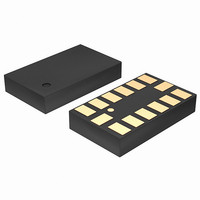
Manufacturer Part Number
ADXL345BCCZ-RL7
Description
Digital Output Three-Axis XL 1500pc RL
Manufacturer
Analog Devices Inc
Series
iMEMS®r
Datasheet
1.EVAL-ADXL345Z.pdf
(40 pages)
Specifications of ADXL345BCCZ-RL7
Design Resources
Sensing Low-g Acceleration Using ADXL345 Digital Accelerometer Connected to ADuC7024 (CN0133)
Axis
X, Y, Z
Acceleration Range
±2g, 4g, 8g, 16g
Sensitivity
256LSB/g, 128LSB/g, 64LSB/g, 32LSB/g
Voltage - Supply
2 V ~ 3.6 V
Output Type
Digital
Bandwidth
6.25Hz ~ 3.2kHz Selectable
Interface
I²C, SPI
Mounting Type
Surface Mount
Package / Case
14-LGA
Lead Free Status / RoHS Status
Lead free / RoHS Compliant
For Use With
EVAL-ADXL345Z - BOARD EVALUATION FOR ADXL345EVAL-ADXL345Z-S - BOARD SATELLITE FOR ADXL345Z-MEVAL-ADXL345Z-M - BOARD EVAL FOR ADXL345
Lead Free Status / RoHS Status
Lead free / RoHS Compliant
Other names
ADXL345BCCZ-RL7TR
Available stocks
Company
Part Number
Manufacturer
Quantity
Price
Company:

Part Number:
ADXL345BCCZ-RL7
Manufacturer:
POWER
Quantity:
14 300


Overrun
The overrun bit is set when new data replaces unread data. The
precise operation of the overrun function depends on the FIFO
mode. In bypass mode, the overrun bit is set when new data replaces
unread data in the DATAX, DATAY, and DATAZ registers (Address
0x32 to Address 0x37). In all other modes, the overrun bit is set
when FIFO is filled. The overrun bit is automatically cleared when
the contents of FIFO are read.
FIFO
The ADXL345 contains patent pending technology for an
embedded memory management system with 32-level FIFO
that can be used to minimize host processor burden. This buffer
has four modes: bypass, FIFO, stream, and trigger (see FIFO Modes).
Each mode is selected by the settings of the FIFO_MODE bits
(Bits[D7:D6]) in the FIFO_CTL register (Address 0x38).
Bypass Mode
In bypass mode, FIFO is not operational and, therefore,
remains empty.
FIFO Mode
In FIFO mode, data from measurements of the x-, y-, and z-axes
are stored in FIFO. When the number of samples in FIFO equals
the level specified in the samples bits of the FIFO_CTL register
(Address 0x38), the watermark interrupt is set. FIFO continues
accumulating samples until it is full (32 samples from measurements
of the x-, y-, and z-axes) and then stops collecting data. After FIFO
stops collecting data, the device continues to operate; therefore,
features such as tap detection can be used after FIFO is full. The
watermark interrupt continues to occur until the number of
samples in FIFO is less than the value stored in the samples bits
of the FIFO_CTL register.
Stream Mode
In stream mode, data from measurements of the x-, y-, and z-
axes are stored in FIFO. When the number of samples in FIFO
equals the level specified in the samples bits of the FIFO_CTL
register (Address 0x38), the watermark interrupt is set. FIFO
continues accumulating samples and holds the latest 32 samples
from measurements of the x-, y-, and z-axes, discarding older
data as new data arrives. The watermark interrupt continues
occurring until the number of samples in FIFO is less than the
value stored in the samples bits of the FIFO_CTL register.
Rev. B | Page 21 of 40
Trigger Mode
In trigger mode, FIFO accumulates samples, holding the latest
32 samples from measurements of the x-, y-, and z-axes. After
a trigger event occurs and an interrupt is sent to the INT1 or
INT2 pin (determined by the trigger bit in the FIFO_CTL register),
FIFO keeps the last n samples (where n is the value specified by
the samples bits in the FIFO_CTL register) and then operates in
FIFO mode, collecting new samples only when FIFO is not full.
A delay of at least 5 μs should be present between the trigger event
occurring and the start of reading data from the FIFO to allow
the FIFO to discard and retain the necessary samples. Additional
trigger events cannot be recognized until the trigger mode is
reset. To reset the trigger mode, set the device to bypass mode
and then set the device back to trigger mode. Note that the FIFO
data should be read first because placing the device into bypass
mode clears FIFO.
Retrieving Data from FIFO
The FIFO data is read through the DATAX, DATAY, and DATAZ
registers (Address 0x32 to Address 0x37). When the FIFO is in
FIFO, stream, or trigger mode, reads to the DATAX, DATAY,
and DATAZ registers read data stored in the FIFO. Each time
data is read from the FIFO, the oldest x-, y-, and z-axes data are
placed into the DATAX, DATAY and DATAZ registers.
If a single-byte read operation is performed, the remaining
bytes of data for the current FIFO sample are lost. Therefore, all
axes of interest should be read in a burst (or multiple-byte) read
operation. To ensure that the FIFO has completely popped (that
is, that new data has completely moved into the DATAX, DATAY,
and DATAZ registers), there must be at least 5 μs between the
end of reading the data registers and the start of a new read of
the FIFO or a read of the FIFO_STATUS register (Address 0x39).
The end of reading a data register is signified by the transition
from Register 0x37 to Register 0x38 or by the CS pin going high.
For SPI operation at 1.6 MHz or less, the register addressing
portion of the transmission is a sufficient delay to ensure that
the FIFO has completely popped. For SPI operation greater than
1.6 MHz, it is necessary to deassert the CS pin to ensure a total
delay of 5 μs; otherwise, the delay is not sufficient. The total delay
necessary for 5 MHz operation is at most 3.4 μs. This is not a
concern when using I
low enough to ensure a sufficient delay between FIFO reads.
2
C mode because the communication rate is
ADXL345
Related parts for ADXL345BCCZ-RL7
Image
Part Number
Description
Manufacturer
Datasheet
Request
R

Part Number:
Description:
±1.7g Dual-Axis IMEMS Accelerometer Evaluation Board
Manufacturer:
Analog Devices Inc
Datasheet:

Part Number:
Description:
Inertial Sensor Evaluation System
Manufacturer:
Analog Devices Inc
Datasheet:
Part Number:
Description:
Manufacturer:
Analog Devices Inc
Datasheet:
Part Number:
Description:
Manufacturer:
Analog Devices Inc
Datasheet:
Part Number:
Description:
Manufacturer:
Analog Devices Inc
Datasheet:
Part Number:
Description:
Manufacturer:
Analog Devices Inc
Datasheet:
Part Number:
Description:
Manufacturer:
Analog Devices Inc
Datasheet:
Part Number:
Description:
Manufacturer:
Analog Devices Inc
Datasheet:
Part Number:
Description:
Manufacturer:
Analog Devices Inc
Datasheet:
Part Number:
Description:
Manufacturer:
Analog Devices Inc
Datasheet:
Part Number:
Description:
Manufacturer:
Analog Devices Inc
Datasheet:
Part Number:
Description:
Manufacturer:
Analog Devices Inc
Datasheet:
Part Number:
Description:
Manufacturer:
Analog Devices Inc
Datasheet: