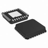
ADN2830ACP32 Analog Devices Inc, ADN2830ACP32 Datasheet - Page 5

ADN2830ACP32
Manufacturer Part Number
ADN2830ACP32
Description
IC,Laser Diode/LED Driver,LLCC,32PIN,PLASTIC
Manufacturer
Analog Devices Inc
Type
Laser Diode Controller (Fiber Optic)r
Datasheet
1.ADN2830ACPZ32.pdf
(12 pages)
Specifications of ADN2830ACP32
Rohs Status
RoHS non-compliant
Number Of Channels
1
Voltage - Supply
4.5 V ~ 5.5 V
Current - Supply
25mA
Current - Bias
200mA
Operating Temperature
-40°C ~ 85°C
Package / Case
32-VFQFN, CSP Exposed Pad
Mounting Type
Surface Mount
Lead Free Status / RoHS Status
GENERAL
Laser diodes have current-in to light-out transfer functions as
shown in Figure 1. Two key characteristics of this transfer func-
tion are the threshold current, I
beyond the threshold current, referred to as slope efficiency (LI).
CONTROL
A monitor photodiode (MPD) is required to control the laser
diode. The MPD current is fed into the ADN2830 to control
the power, continuously adjusting the bias current in response
to the laser’s changing threshold current and light to current
(LI) slope (slope efficiency).
The ADN2830 uses automatic power control (APC) to maintain
a constant power over time and temperature.
The average power is controlled by the R
connected between the PSET pin and ground. The PSET pin
is kept 1.23 V above GND. For an initial setup, the R
tor can be calculated using the following formula.
where I
Note the I
required to know exact values for LI and MPD optical coupling.
LOOP BANDWIDTH SELECTION
Capacitor values greater than 22 nF are used to set the actual
loop bandwidth. This capacitor is placed between the PAVCAP
pin and ground. It is important that the capacitor is a low leak-
age multilayer ceramic with an insulation resistance greater than
100 GΩ or a time constant of 1000 sec, whichever is less.
ALARMS
The ADN2830 has two active high alarms, DEGRADE and
FAIL. A resistor between ground and the ASET pin is used to
set the current at which these alarms are raised. The current
through the ASET resistor is a ratio of (N
alarm threshold (N is the number of ADN2830s in parallel).
The DEGRADE alarm will be raised at 90% of this level.
*The smallest value for R
REV. A
maximum of N
AV
is average MPD current.
PSET
Figure 1. Laser Transfer Function
P
will change from device to device. It is not
200 mA.
AV
ASET
R
is 1.2 kΩ, as this corresponds to the IBIAS
PSET
=
TH
1 23
, and slope in the linear region
.
I
I
TH
AV
V
I
CURRENT
PSET
P
LI =
200):1 to the FAIL
resistor
P
I
PSET
resis-
–5–
Example:
The laser degrade alarm, DEGRADE, gives a warning of imminent
laser failure if the laser diode degrades further or environmental condi-
tions continue to stress the laser diode, e.g., increasing temperature.
The laser fail alarm, FAIL, is activated when:
•
•
DEGRADE will only be raised when the bias current exceeds
90% of the ASET current.
MONITOR CURRENTS
IBMON and IMPDMON are current controlled current sources
from V
monitoring functionality. An external resistor to GND gives a
voltage proportional to the current monitored. If the IMPDMON
function is not used, the IMPD pin must be grounded and the
monitor photodiode must be tied directly to the PSET pin.
AUTOMATIC LASER SHUTDOWN
When ALS is logic high, the bias current is turned off. Correct
operation of ALS can be confirmed by the fail alarm being
raised when ALS is asserted. Note that this is the only time
DEGRADE will be low while FAIL is high.
MODE
The MODE feature on the ADN2830 allows the user to operate
more than one ADN2830 in parallel current boosting mode to
achieve up to N
ADN2830s in parallel). When using parallel boosting mode, one
device is run as the master, the other as the slave. The MODE
pin on the master is tied to ALS and the MODE pin on the
slave is tied high (see Figure 3 for reference circuit).
ALARM INTERFACES
The FAIL and DEGRADE outputs have an internal 30 kΩ
pull-up resistor that is used to pull the digital high value to V
However, the alarm output may be overdriven with an external
resistor allowing the alarm interfacing to non-V
Non-V
the ADN2830.
The ASET threshold is reached.
The ALS pin is set high. This shuts off the modulation and
bias currents to the laser diode, resulting in the MPD current
dropping to zero.
CC
CC
. They mirror the bias and MPD current for increased
alarm output levels must be below the V
I
FAIL
*R
I
ASET
ASET
=
50
200 mA of bias current (N is the number of
=
=
mA N
N
I
1 23
BIASTRIP
I
.
ASET
×
,
200
V
= ∴
=
1
=
250
50
1 23
I
200
.
DEGRADE
mA
µ
A
=
=
4 92
250
.
=
ADN2830
CC
45
µ
k
CC
A
levels.
Ω
mA
used for
CC.


