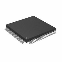
AD9878BSTZ Analog Devices Inc, AD9878BSTZ Datasheet - Page 17

AD9878BSTZ
Manufacturer Part Number
AD9878BSTZ
Description
IC,MODEM CIRCUIT,ANALOG FRONT END,CMOS,QFP,100PIN,PLASTIC
Manufacturer
Analog Devices Inc
Datasheet
1.AD9878BSTZ.pdf
(36 pages)
Specifications of AD9878BSTZ
Number Of Bits
12
Number Of Channels
4
Power (watts)
673mW
Voltage - Supply, Analog
3.3V
Voltage - Supply, Digital
3.3V
Package / Case
100-LQFP
Lead Free Status / RoHS Status
Lead free / RoHS Compliant
Available stocks
Company
Part Number
Manufacturer
Quantity
Price
Company:
Part Number:
AD9878BSTZ
Manufacturer:
ADI
Quantity:
328
Company:
Part Number:
AD9878BSTZ
Manufacturer:
Analog Devices Inc
Quantity:
10 000
Part Number:
AD9878BSTZ
Manufacturer:
ADI/亚德诺
Quantity:
20 000
Setting this bit to 0 (default) configures the serial interface to be
compatible with AD8321/AD8323/AD8328 variable cable gain
amplifiers. Setting this bit to 1 configures the serial interface to be
compatible with AD8322/AD8327 variable cable gain amplifiers.
Bit 5: Profile Select
The AD9878 quadrature digital upconverter can store two
preconfigured modulation modes, called profiles. Each profile
defines a transmit FTW, cable-driver amplifier gain setting, and
DAC gain setting. The profile select bit or PROFILE pin programs
the current register profile to be used. If the PROFILE pin is used
to switch between profiles, the profile select bit should be set to 0
and tied low.
REGISTERS 0x10 THROUGH 0x17—
BURST PARAMETER
Tx Frequency Tuning Words
The FTW determines the DDS-generated carrier frequency (f
and is formed via a concatenation of register addresses.
The 26-bit FTW is spread over four register addresses. Bit 25 is
the MSB, and Bit 0 is the LSB. The carrier frequency equation is
as follows:
Where
Changes to FTW bytes take effect immediately.
Cable-Driver Gain Control
The AD9878 has a 3-pin interface to the AD832x family of
programmable gain cable-driver amplifiers. This allows direct
control of the cable driver’s gain through the AD9878. In its
default mode, the complete 8-bit register value is transmitted
over the 3-wire cable amplifier (CA) interface.
If Bit 3 of Register 0x0F is set high, Bits [7:4] of Register 0x13
and Register 0x17 determine the 8-bit word sent over the CA
interface, according to the specifications in Table 6. Bits [3:0] of
Register 0x13 and Register 0x17 determine the fine gain setting
of the DAC output, according to specifications in Table 7.
f
C
f
=
SYSCLK
(
FTW
=
×
M
f
SYSCLK
×
f
OSCIN
)
2
,
26
and
FTW
<
x 0
2000
.
Rev. A | Page 17 of 36
C
)
Table 6. Cable-Driver Gain Control
Bits [7:4]
0000
0001
0010
0011
0100
0101
0110
0111
1000
Table 7. DAC Output Fine Gain Setting
Bits [3:0]
0000
0001
0010
0011
…
1110
1111
New data is automatically sent over the 3-wire CA interface
(and DAC gain adjust) whenever the value of the active gain
control register changes or a new profile is selected. The default
value is 0x00 (lowest gain).
The formula for the combined output-level calculation of
AD9878 fine gain and AD8327 or AD8322 coarse gain is:
where:
fine is the decimal value of Bits [3:0].
coarse is the decimal value of Bits [7:4].
V
V
V
9878(0)
8327
8322
V
V
is the level at output of AD8327 in dBmV.
is the level at output of AD8322 in dBmV.
8327
8322
is the level at AD9878 output in dBmV for fine = 0.
=
=
V
V
9878
9878
( )
( )
0
0
CA Interface Transmit Word
0000 0000 (default)
0000 0001
0000 0010
0000 0100
0000 1000
0001 0000
0010 0000
0100 0000
1000 0000
+
+
(
(
DAC Fine Gain (dB)
0.0 (default)
0.5
1.0
1.5
…
7.0
7.5
fine
fine
)
)
2
2
+
+
(
(
coarse
coarse
)
)
−
−
19
14
AD9878


