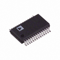
AD7899ARSZ-2 Analog Devices Inc, AD7899ARSZ-2 Datasheet - Page 12

AD7899ARSZ-2
Manufacturer Part Number
AD7899ARSZ-2
Description
14-BIT BIPOLAR INPUT SINGLE SUPPLY ADC
Manufacturer
Analog Devices Inc
Datasheet
1.AD7899ARSZ-1.pdf
(16 pages)
Specifications of AD7899ARSZ-2
Number Of Bits
14
Sampling Rate (per Second)
400k
Data Interface
Parallel
Number Of Converters
1
Power Dissipation (max)
125mW
Voltage Supply Source
Single Supply
Operating Temperature
-40°C ~ 85°C
Mounting Type
Surface Mount
Package / Case
28-SSOP (0.200", 5.30mm Width)
Number Of Elements
1
Resolution
14Bit
Architecture
SAR
Sample Rate
400KSPS
Input Polarity
Unipolar
Input Type
Voltage
Rated Input Volt
2.5/5V
Differential Input
No
Power Supply Requirement
Single
Single Supply Voltage (typ)
5V
Single Supply Voltage (min)
4.75V
Single Supply Voltage (max)
5.25V
Dual Supply Voltage (typ)
Not RequiredV
Dual Supply Voltage (min)
Not RequiredV
Dual Supply Voltage (max)
Not RequiredV
Power Dissipation
125mW
Differential Linearity Error
±1LSB
Integral Nonlinearity Error
±2LSB
Operating Temp Range
-40C to 85C
Operating Temperature Classification
Industrial
Mounting
Surface Mount
Pin Count
28
Package Type
SSOP
Input Signal Type
Single-Ended
Lead Free Status / RoHS Status
Lead free / RoHS Compliant
For Use With
EVAL-AD7899CBZ - BOARD EVAL FOR AD7899
Lead Free Status / Rohs Status
Compliant
Available stocks
Company
Part Number
Manufacturer
Quantity
Price
Part Number:
AD7899ARSZ-2
Manufacturer:
ADI/亚德诺
Quantity:
20 000
AD7899
Standby Mode Operation
The AD7899 has a Standby Mode whereby the device can be
placed in a low current consumption mode (5 µA typ). The
AD7899 is placed in Standby by bringing the logic input STBY
low. The AD7899 can be powered again up for normal opera-
tion by bringing STBY logic high. The output data buffers are
still operational while the AD7899 is in Standby. This means
the user can still continue to access the conversion results while
the AD7899 is in standby. This feature can be used to reduce
the average power consumption in a system using low throughput
rates. To reduce the average power consumption, the AD7899
can be placed in standby at the end of each conversion sequence
and taken out of standby again prior to the start of the next
conversion sequence. The time it takes the AD7899 to come out
of standby is called the “wake up” time. This wake-up time will
limit the maximum throughput rate at which the AD7899 can
be operated when powering down between conversions. When
the AD7899 is used with the internal reference, the reference
capacitor will begin to discharge during standby. The voltage
remaining on the capacitor at wake-up time will depend upon
the standby time and hence affect the wake-up time. The mini-
mum wake-up time is typically 2 µs. The maximum wake-up
time will be when the AD7899 has been in standby long enough
for the reference capacitor to fully discharge. The wake-up time
in this case will typically be 15 ms. The AD7899 will wake up in
approximately 1 µs when using an external reference, regardless
of sleep time.
When operating the AD7899 in a Standby mode between con-
versions, the power savings can be significant. For example,
with a throughput rate of 10 kSPS and an external reference, the
AD7899 will be powered up for 4.2 µs out of every 100 µs (2 µs
for wake-up time and 2.2 µs for conversion time). Therefore, the
average power consumption drops to 80 mW × 4.2% or approxi-
mately 3.36 mW.
AD7899 DYNAMIC SPECIFICATIONS
The AD7899 is specified and 100% tested for dynamic perfor-
mance specifications as well as traditional dc specifications such
as Integral and Differential Nonlinearity. These ac specifications
are required for the signal processing applications such as phased
array sonar, adaptive filters, and spectrum analysis. These appli-
cations require information on the ADC’s effect on the spectral
content of the input signal. Hence, the parameters for which the
AD7899 is specified include SNR, harmonic distortion, inter-
modulation distortion, and peak harmonics. These terms are
discussed in more detail in the following sections.
CONVST/
CLKIN
EOC
1
(INPUT SAMPLED)
START OF NEW
CONVERSION
2
3
4
5
6
7
Signal-to-Noise Ratio (SNR)
SNR is the measured signal-to-noise ratio at the output of the
ADC. The signal is the rms magnitude of the fundamental.
Noise is the rms sum of all the nonfundamental signals up to
half the sampling frequency (f
upon the number of quantization levels used in the digitization
process; the more levels, the smaller the quantization noise. The
theoretical signal to noise ratio for a sine wave input is given by
where N is the number of bits.
Thus for an ideal 14-bit converter, SNR = 86.04 dB.
Figure 9 shows a histogram plot for 8192 conversions of a dc
input using the AD7899 with 5 V supply. The analog input was
set at the center of a code transition. It can be seen that most of
the codes appear in one output bin, indicating very good noise
performance from the ADC.
The output spectrum from the ADC is evaluated by applying a
sine wave signal of very low distortion to the analog input. A
Fast Fourier Transform (FFT) plot is generated from which the
SNR data can be obtained. Figure 10 shows a typical 4096 point
FFT plot of the AD7899 with an input signal of 100 kHz and a
sampling frequency of 400 kHz. The SNR obtained from this
graph is 80.5 dB. It should be noted that the harmonics are
taken into account when calculating the SNR.
8
SNR = (6.02N + 1.76) dB
7000
6000
5000
4000
3000
2000
1000
9
0
10
11
CONVERSION
COMPLETE
12
S
/2) excluding dc. SNR is dependent
13
14
15
16
(1)


