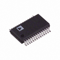
AD7862ARSZ-2 Analog Devices Inc, AD7862ARSZ-2 Datasheet - Page 5

AD7862ARSZ-2
Manufacturer Part Number
AD7862ARSZ-2
Description
DUAL 12-BIT PARALLEL ADC I.C.
Manufacturer
Analog Devices Inc
Datasheet
1.AD7862ARZ-10.pdf
(16 pages)
Specifications of AD7862ARSZ-2
Number Of Bits
12
Sampling Rate (per Second)
250k
Data Interface
Parallel
Number Of Converters
2
Power Dissipation (max)
75mW
Voltage Supply Source
Analog and Digital
Operating Temperature
-40°C ~ 85°C
Mounting Type
Surface Mount
Package / Case
28-SSOP (0.200", 5.30mm Width)
Lead Free Status / RoHS Status
Lead free / RoHS Compliant
Available stocks
Company
Part Number
Manufacturer
Quantity
Price
Part Number:
AD7862ARSZ-2
Manufacturer:
ADI/亚德诺
Quantity:
20 000
Pin
1
2
3–6
7
8
9–15
16
17
18
19
20
21
22
23
24
25
26
27
28
REV. 0
Mnemonic
NC
DB11
DB10–DB7
DGND
CONVST
DB6–DB0
AGND
V
V
VREF
A0
CS
RD
BUSY
VDD
V
V
AGND
NC
B2
A2
A1
B1
Description
No Connect
Data Bit 11 (MSB). Three-state TTL output. Output coding is twos complement for the AD7862-
10 and AD7862-3. Output coding is straight (natural) binary for the AD7862-2.
Data Bit 10 to Data Bit 7. Three-state TTL outputs.
Digital Ground. Ground reference for digital circuitry.
Convert Start Input. Logic Input. A high to low transition on this input puts both track/holds into
their hold mode and starts conversion on both channels.
Data Bit 6 to Data Bit 0. Three-state TTL outputs.
Analog Ground. Ground reference for mux, track/hold, reference and DAC circuitry.
Input Number 2 of Channel B. Analog Input voltage ranges of
(AD7862-3) and 0 V–2.5 V (AD7862-2).
Input Number 2 of Channel A. Analog Input voltage ranges of 10 V (AD7862-10), 2.5 V
(AD7862-3) and 0 V–2.5 V (AD7862-2).
Reference Input/Output. This pin is connected to the internal reference through a series resistor and is
the output reference source for the analog-to-digital converter. The nominal reference voltage is 2.5 V,
and this appears at the pin.
Multiplexer Select. This input is used in conjunction with RD and CS low to enable the data outputs.
With A0 logic low, one read after a conversion will read the data from each of the ADCs in the sequence,
V
Chip Select Input. Active low logic input. The device is selected when this input is active.
Read Input. Active low logic input. This input is used in conjunction with A0 and CS low to enable
the data outputs. With A0 logic low, one read after a conversion will read the data from each of the
ADCs in the sequence, V
V
Busy Output. The busy output is triggered high by the falling edge of CONVST and remains high
until conversion is completed.
Analog and Digital Positive Supply Voltage, +5.0 V
Input Number 1 of Channel A. Analog Input voltage ranges of 10 V (AD7862-10), 2.5 V
(AD7862-3) and 0 V–2.5 V (AD7862-2).
Input Number 1 of Channel B. Analog Input voltage ranges of
(AD7862-3) and 0 V–2.5 V (AD7862-2).
Analog Ground. Ground reference for mux, track/hold, reference and DAC circuitry.
No Connect
A1
B2
, V
.
A2
, and a subsequent read, when A0 goes high, reads the data from V
PIN FUNCTION DESCRIPTION
CONVST
PIN CONFIGURATION
DGND
A1
DB11
DB10
DB9
DB8
DB7
DB6
DB5
DB4
DB3
DB2
DB1
NC
, V
10
11
12
13
14
A2
1
2
3
4
5
6
7
8
9
NC = NO CONNECT
, and a subsequent read, when A0 goes high, reads the data from V
(Not to Scale)
AD7862
TOP VIEW
–5–
28
27
26
25
24
23
22
21
20
19
18
17
16
15
NC
AGND
V
V
V
BUSY
RD
CS
A0
V
V
V
AGND
DB0
B1
A1
DD
REF
A2
B2
5%.
10 V (AD7862-10), 2.5 V
10 V (AD7862-10), 2.5 V
B1
, V
B2
.
AD7862
B1,


