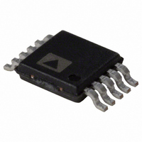
AD7685CRMZRL7 Analog Devices Inc, AD7685CRMZRL7 Datasheet - Page 5

AD7685CRMZRL7
Manufacturer Part Number
AD7685CRMZRL7
Description
IC,A/D CONVERTER,SINGLE,16-BIT,CMOS,TSSOP,10PIN
Manufacturer
Analog Devices Inc
Series
PulSAR®r
Datasheet
1.AD7685BCPZRL7.pdf
(28 pages)
Specifications of AD7685CRMZRL7
Design Resources
Parametric Measurement Unit and Supporting Components for PAD Appls Using AD5522 and AD7685 (CN0104) Integrated Device Power Supply for PAD with Output Voltage Range 0 V to 25 V (CN0130)
Number Of Bits
16
Sampling Rate (per Second)
250k
Data Interface
DSP, MICROWIRE™, QSPI™, Serial, SPI™
Number Of Converters
1
Power Dissipation (max)
15mW
Voltage Supply Source
Single Supply
Operating Temperature
-40°C ~ 85°C
Mounting Type
Surface Mount
Package / Case
10-TFSOP (0.118", 3.00mm Width)
Lead Free Status / RoHS Status
Lead free / RoHS Compliant
For Use With
EVAL-AD7685CBZ - BOARD EVAL FOR AD7685
Lead Free Status / RoHS Status
Lead free / RoHS Compliant
Available stocks
Company
Part Number
Manufacturer
Quantity
Price
Part Number:
AD7685CRMZRL7
Manufacturer:
ADI/亚德诺
Quantity:
20 000
TIMING SPECIFICATIONS
−40°C to +85°C, VIO = 2.3 V to 5.5 V or VDD + 0.3 V, whichever is the lowest, unless otherwise stated.
Table 4. VDD = 4.5 V to 5.5 V
Parameter
Conversion Time: CNV Rising Edge To Data Available
Acquisition Time
Time Between Conversions
CNV Pulse Width (CS Mode)
SCK Period (CS Mode)
SCK Period (Chain Mode)
SCK Low Time
SCK High Time
SCK Falling Edge to Data Remains Valid
SCK Falling Edge to Data Valid Delay
CNV or SDI Low to SDO D15 MSB Valid (CS Mode)
CNV or SDI High or Last SCK Falling Edge to SDO High Impedance (CS Mode)
SDI Valid Setup Time from CNV Rising Edge (CS Mode)
SDI Valid Hold Time from CNV Rising Edge (CS Mode)
SCK Valid Setup Time from CNV Rising Edge (Chain Mode)
SCK Valid Hold Time from CNV Rising Edge (Chain Mode)
SDI Valid Setup Time from SCK Falling Edge (Chain Mode)
SDI Valid Hold Time from SCK Falling Edge (Chain Mode)
SDI High to SDO High (Chain Mode with Busy Indicator)
1
See Figure 3 and Figure 4 for load conditions.
VIO Above 4.5 V
VIO Above 3 V
VIO Above 2.7 V
VIO Above 2.3 V
VIO Above 4.5 V
VIO Above 3 V
VIO Above 2.7 V
VIO Above 2.3 V
VIO Above 4.5 V
VIO Above 2.7 V
VIO Above 2.3 V
VIO Above 4.5 V
VIO Above 2.3 V
1
Rev. B | Page 5 of 28
Symbol
t
t
t
t
t
t
t
t
t
t
t
t
t
t
t
t
t
t
t
CONV
ACQ
CYC
CNVH
SCK
SCK
SCKL
SCKH
HSDO
DSDO
EN
DIS
SSDICNV
HSDICNV
SSCKCNV
HSCKCNV
SSDISCK
HSDISCK
DSDOSDI
Min
0.5
1.8
4
10
15
17
18
19
20
7
7
5
15
0
5
5
3
4
Typ
Max
2.2
14
15
16
17
15
18
22
25
15
26
AD7685
Unit
μs
μs
μs
ns
ns
ns
ns
ns
ns
ns
ns
ns
ns
ns
ns
ns
ns
ns
ns
ns
ns
ns
ns
ns
ns
ns
ns
ns


