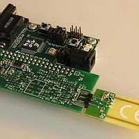
MC33696MOD315EV Freescale Semiconductor, MC33696MOD315EV Datasheet - Page 13

MC33696MOD315EV
Manufacturer Part Number
MC33696MOD315EV
Description
MCU, MPU & DSP Development Tools MC33696 (ECHO) RF C EVAL
Manufacturer
Freescale Semiconductor
Datasheet
1.MC33696MOD868EV.pdf
(80 pages)
Specifications of MC33696MOD315EV
Processor To Be Evaluated
MC9S08RG60
Interface Type
RS-232
Lead Free Status / RoHS Status
Lead free / RoHS Compliant
- Current page: 13 of 80
- Download datasheet (2Mb)
12
The receiver is either waiting for an RF transmission or is receiving one. Two different processes are
possible, as determined by the values of the DME bit. The transmitter part is kept off. A state diagram
describes the sequence of operations in each case.
12.1 Data Manager Disabled (DME=0)
Data manager disabled means that the SPI is deselected and raw data is sent directly on the MOSI line,
while SCLK remains at low level.
Two different processes are possible, as determined by the values of the SOE bit.
12.1.1 Data Manager Disabled and Strobe Pin Control
Raw received data is sent directly on the MOSI line.
For all states: At any time, a low level applied to CONFB forces the state machine to state 1, configuration
mode.
Freescale Semiconductor
•
•
State 5:
The receiver is in standby/LVD mode. For further information, see
Mode.” A high level applied to STROBE forces the circuit to state 5b.
State 5b:
The receiver is kept on by the STROBE pin. Raw data is output on the MOSI line.
Receive Mode
If the STROBE pin is tied to a high level before switching to receive mode,
the receiver does not go through an off or standby state.
STROBE = 1
Figure 3. Receive Mode, DME = 0, SOE = 0
MC33696 Data Sheet, Rev. 12
Raw Data on MOSI
Standby/LVD
State 5b
State 5
NOTE
On
STROBE = 0
STROBE = 1
Figure 3
shows the state diagram.
STROBE = 0
Section 14, “Standby: LVD
SPI Deselected
Receive Mode
13
Related parts for MC33696MOD315EV
Image
Part Number
Description
Manufacturer
Datasheet
Request
R
Part Number:
Description:
Manufacturer:
Freescale Semiconductor, Inc
Datasheet:
Part Number:
Description:
Manufacturer:
Freescale Semiconductor, Inc
Datasheet:
Part Number:
Description:
Manufacturer:
Freescale Semiconductor, Inc
Datasheet:
Part Number:
Description:
Manufacturer:
Freescale Semiconductor, Inc
Datasheet:
Part Number:
Description:
Manufacturer:
Freescale Semiconductor, Inc
Datasheet:
Part Number:
Description:
Manufacturer:
Freescale Semiconductor, Inc
Datasheet:
Part Number:
Description:
Manufacturer:
Freescale Semiconductor, Inc
Datasheet:
Part Number:
Description:
Manufacturer:
Freescale Semiconductor, Inc
Datasheet:
Part Number:
Description:
Manufacturer:
Freescale Semiconductor, Inc
Datasheet:
Part Number:
Description:
Manufacturer:
Freescale Semiconductor, Inc
Datasheet:
Part Number:
Description:
Manufacturer:
Freescale Semiconductor, Inc
Datasheet:
Part Number:
Description:
Manufacturer:
Freescale Semiconductor, Inc
Datasheet:
Part Number:
Description:
Manufacturer:
Freescale Semiconductor, Inc
Datasheet:
Part Number:
Description:
Manufacturer:
Freescale Semiconductor, Inc
Datasheet:
Part Number:
Description:
Manufacturer:
Freescale Semiconductor, Inc
Datasheet:


