MC33696MOD868EV Freescale Semiconductor, MC33696MOD868EV Datasheet - Page 24

MC33696MOD868EV
Manufacturer Part Number
MC33696MOD868EV
Description
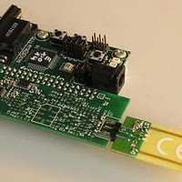
MCU, MPU & DSP Development Tools MC33696 (ECHO) RF C EVAL
Manufacturer
Freescale Semiconductor
Datasheet
1.MC33696MOD868EV.pdf
(80 pages)
Specifications of MC33696MOD868EV
Processor To Be Evaluated
MC9S08RG60
Interface Type
RS-232
Lead Free Status / RoHS Status
Lead free / RoHS Compliant
Receive Mode
Therefore, the logarithmic amplifier provides information relative to the in-band signal, whereas the LNA
AGC voltage senses the input signal over a wider band.
The RSSI information given by the logarithmic amplifier is available in:
The information from the LNA AGC is available in digital form in the four most significant bits of status
register RSSI.
The whole content of status register RSSI provides 2 ¥ 4 bits of RSSI information about the incoming
signal (see
Figure 15
The quasi peak detector (D1, R1, C1) has a charge time of about 20 μs to avoid sensitivity to spikes.
R2 controls the decay time constant of about 5 ms to allow efficient smoothing of the OOK modulated
signal at low data rates. This time constant is useful in continuous mode when S2 is permanently closed.
To allow high-speed RSSI updating in peak pulse measurement, a discharge circuit (S1) is required to reset
the measured voltage and to allow new peak detection.
S2 is used to sample the RSSI voltage to allow peak pulse measurement (S2 used as sample and hold), or
to allow continuous transparent measurement (S2 continuously closed).
The 4-bit analog-to-digital convertor (ADC) is based on a flash architecture. The conversion time is
16 × T
on a 32 × T
If RSSIE is reset, the whole RSSI module is switched off, reducing the current consumption. The output
buffer connected to RSSIOUT is set to high impedance.
24
IF Filter Output
•
•
•
diglck
At the LNA output, the LNA AGC control voltage is used to monitor input signals in the range
–50 dBm to –20 dBm.
Analog form on pin RSSIOUT
Digital form in the four least significant bits of the status register RSSI
shows a simplified block diagram of the RSSI function.
Section 18.6, “RSSI
digclk
. As a single convertor is used for the two analog signals, the RSSI register content is updated
timebase.
Register”).
Figure 15. RSSI Simplified Block Diagram
Σ
MC33696 Data Sheet, Rev. 12
LNA AGC Out
D1
R1
C1
R2
S1
ADC
Freescale Semiconductor
MSB
S2
C2
RSSI Register
RSSIOUT
LSB


