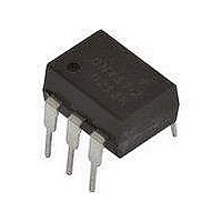
H11N3FR2VM Fairchild Semiconductor, H11N3FR2VM Datasheet - Page 3

H11N3FR2VM
Manufacturer Part Number
H11N3FR2VM
Description
High Speed Optocouplers 6-Pin Octocoupler
Manufacturer
Fairchild Semiconductor
Datasheet
1.H11N3TM.pdf
(9 pages)
Specifications of H11N3FR2VM
Isolation Voltage
5300 Vrms
Maximum Continuous Output Current
50 mA
Maximum Fall Time
12 ns
Maximum Forward Diode Current
30 mA
Maximum Rise Time
7.5 ns
Output Device
Logic Gate Photo IC
Configuration
1 Channel
Maximum Baud Rate
5 MBps
Maximum Forward Diode Voltage
2 V
Maximum Reverse Diode Voltage
6 V
Maximum Power Dissipation
250 mW
Maximum Operating Temperature
+ 85 C
Minimum Operating Temperature
- 40 C
Package / Case
PDIP-6
Lead Free Status / RoHS Status
Lead free / RoHS Compliant
© 2005 Fairchild Semiconductor Corporation
*Typical values at T
NOTES:
1. Maximum I
2. H11N1: R
TRANSFER CHARACTERISTICS
DC Characteristics
Supply Current
Output Voltage, low
Turn-On Threshold Current
Turn-Off Threshold Current
Hysteresis Ratio
AC Characteristics
Propagation delay time
High to Low
Rise Time
Propagation delay time
Low to High
Fall time
Data Rate
ISOLATION CHARACTERISTICS
Parameters
Input-Output Isolation Voltage
Isolation Capacitance
Isolation Resistance
SWITCHING SPEED
H11N1-M
require the LED to be driven at a current greater than 3.2mA to guarantee the device will turn on. A 10% guard band is
recommended to account for degradation of the LED over its lifetime. The maximum allowable LED drive current is 30mA.
H11N2: R
H11N3: R
E
E
E
F(ON)
= 910 Ω
= 560 Ω
= 240 Ω
A
is the maximum current required to trigger the output. For example, a 3.2mA maximum trigger current would
= 25°C
I
R
R
note 1
R
R
C=120pF, t
Fig. 1
C=120pF, t
Fig. 1
C=120pF, t
Fig. 1
C=120pF, t
Fig. 1
F
L
L
L
L
= 10mA, V
=270 Ω ,V
=270 Ω , V
=270 Ω , V
=270 Ω , V
V
V
f = 60 Hz, t =1 sec.
I-O
I-O
Test Conditions
Test Conditions
Test Conditions
= 0V, f = 1 MHz
= ±500 VDC
P
P
P
P
CC
CC
CC
CC
=1µs, R
=1µs, R
=1µs, R
=1µs, R
CC
HIGH SPEED LOGIC OPTOCOUPLERS
=5V, I
= 5V
= 5V
= 5V
= 5V
F
E
E
E
E
=I
: Note 2
: Note 2
: Note 2
: Note 2
F(on)
H11N2-M
Page 3 of 9
max.
Symbol
C
R
V
I
F(off)
Symbol
Symbol
ISO
ISO
ISO
I
CC(on)
I
I
t
t
V
F(on)
F(off)
PHL
PLH
t
OL
t
/I
r
f
F(on)
7500
H11N1-M
H11N2-M
H11N3-M
10
Min
Device
Device
11
All
All
All
All
All
All
All
All
All
Typ*
0.65
Min
Min
0.4
0.8
2.3
4.1
0.3
Typ*
100
150
Typ
6.5
7.5
12
5
Max
0.6
6-PIN DIP
H11N3-M
0.95
Max
Max
330
330
0.5
3.2
10
10
5
V
Units
6/15/05
PEAK
pF
Ω
Units
Units
MHz
mA
mA
mA
ns
ns
ns
ns
V


