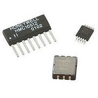
HMC6352 Honeywell Microelectronics & Precision Sensors, HMC6352 Datasheet - Page 3

HMC6352
Manufacturer Part Number
HMC6352
Description
Magnetic Sensor
Manufacturer
Honeywell Microelectronics & Precision Sensors
Datasheet
1.HMC6352.pdf
(13 pages)
Specifications of HMC6352
Msl
MSL 3 - 168 Hours
Terminal Type
PCB
Supply Voltage
5.2V
Sensor Terminals
SMD
Supply Current
10mA
Magnetic Field Max
0.75G
Axis Configuration
Two
Magnetic Field Min
0.10G
Available stocks
Company
Part Number
Manufacturer
Quantity
Price
Company:
Part Number:
HMC6352
Manufacturer:
honeywell
Quantity:
12 800
Part Number:
HMC6352
Manufacturer:
HITTITE
Quantity:
20 000
Company:
Part Number:
HMC6352-TR
Manufacturer:
HIROSE
Quantity:
670
HMC6352
Pin Descriptions
HMC6352
I
The HMC6352 communicates via a two-wire I
with the interface protocol defined by the I
The data rate is the standard-mode 100kbps rate as defined in the I
Data/Address send and a 1-bit acknowledge bit. The format of the data bytes (payload) shall be case sensitive ASCII
characters or binary data to the HMC6352 slave, and binary data returned. Negative binary values will be in two’s
complement form. The default (factory) HMC6352 7-bit slave address is 42(hex) for write operations, or 43(hex) for read
operations.
The HMC6352 Serial Clock (SCL) and Serial Data (SDA) lines do not have internal pull-up resistors, and require resistive
pull-ups (Rp) between the master device (usually a host microprocessor) and the HMC6352. Pull-up resistance values of
about 10k ohms are recommended with a nominal 3.0-volt supply voltage. Other values may be used as defined in the I
Bus Specification 2.1.
The SCL and SDA lines in this bus specification can be connected to a host of devices. The bus can be a single master to
multiple slaves, or it can be a multiple master configuration. All data transfers are initiated by the master device which is
responsible for generating the clock signal, and the data transfers are 8 bit long. All devices are addressed by I
unique 7 bit address. After each 8-bit transfer, the master device generates a 9
The receiving device (addressed slave) will pull the SDA line low to acknowledge (ACK) the successful transfer or leave
the SDA high to negative acknowledge (NACK).
Per the I
conditions on the bus associated with the SDA transitions when SCL is high. Master device pulling the SDA line low while
the SCL line is high indicates the Start (S) condition, and the Stop (P) condition is when the SDA line is pulled high while
the SCL line is high. The I
start condition without issuing a stop.
All bus transactions begin with the master device issuing the start sequence followed by the slave address byte. The
address byte contains the slave address; the upper 7 bits (bits7-1), and the Least Significant bit (LSb). The LSb of the
www.honeywell.com
2
Pin
10
11
12
13
14
15
16
17
18
19
20
21
22
23
24
1
2
3
4
5
6
7
8
9
C Communication Protocol
2
Name
OF-
SR+
NC
NC
GND
NC
SDI
SDO
PGM
SCL
SS
NC
NC
VDD
NC
NC
NC
NC
CB2
CB1
NC
CA2
CA1
OF+
C spec, all transitions in the SDA line must occur when SCL is low. This requirement leads to two unique
2
C protocol also allows for the Restart condition in which the master device issues a second
Description
No User Connection (Offset Strap Negative)
No User Connection (Set/Reset Strap Positive)
No User Connection
No User Connection
Supply/System Ground
No User Connection
I2C Data Output (SPI Data In)
No User Connection (SPI Data Out)
No User Connection (Program Enable)
I2C Clock (SPI Clock)
No User Connection (Slave Select)
No User Connection
No User Connection
Supply Voltage Positive Input (+2.7VDC to +5.0VDC)
No User Connection
No User Connection
No User Connection
No User Connection
Amplifier B Filter Capacitor Connection
Amplifier B Filter Capacitor Connection
No User Connection
Amplifier A Filter Capacitor Connection
Amplifier A Filter Capacitor Connection
No User Connection (Offset Strap Positive)
2
C bus specification, and the lower command protocol defined by Honeywell.
2
C bus system as a slave device. The HMC6352 uses a layered protocol
2
C Bus Specification 2.1. The bus bit format is an 8-bit
th
clock pulse, and releases the SDA line.
2
C’s
3
2
C


