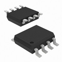
AD22100AR Analog Devices Inc, AD22100AR Datasheet - Page 7

AD22100AR
Manufacturer Part Number
AD22100AR
Description
IC TEMP SENSOR VOUT 8-SOIC
Manufacturer
Analog Devices Inc
Datasheet
1.AD22100ARZ.pdf
(12 pages)
Specifications of AD22100AR
Rohs Status
RoHS non-compliant
Sensing Temperature
-50°C ~ 150°C
Output Type
Voltage
Voltage - Supply
4 V ~ 6.5 V
Accuracy
±1°C
Package / Case
8-SOIC (0.154", 3.90mm Width)
Peak Reflow Compatible (260 C)
No
Ic Function
Temperature Sensor IC
Leaded Process Compatible
No
Mounting Type
Surface Mount
Operating Temperature Range
-50°C To +150°C
Operating Temperature Min
-40°C
Lead Free Status / RoHS Status
Contains lead / RoHS non-compliant
Available stocks
Company
Part Number
Manufacturer
Quantity
Price
Part Number:
AD22100AR
Manufacturer:
ADI/亚德诺
Quantity:
20 000
Part Number:
AD22100ARZ
Manufacturer:
ADI/亚德诺
Quantity:
20 000
Company:
Part Number:
AD22100ARZ-RL
Manufacturer:
FREESCALE
Quantity:
6 218
THEORY OF OPERATION
The AD22100 is a ratiometric temperature sensor IC whose
output voltage is proportional to its power supply voltage. The
heart of the sensor is a proprietary temperature-dependent
resistor, similar to an RTD, which is built into the IC. Figure 7
shows a functional block diagram of the AD22100.
The temperature-dependent resistor, labeled R
change in resistance that is nearly linearly proportional to
temperature. This resistor is excited with a current source that is
proportional to the power supply voltage. The resulting voltage
across R
arly varying with temperature. The remainder of the AD22100
consists of an op amp signal conditioning block that takes the
voltage across R
achieve the following output voltage function:
ABSOLUTE ACCURACY AND NONLINEARITY
SPECIFICATIONS
Figure 8 graphically depicts the guaranteed limits of accuracy
for the AD22100 and shows the performance of a typical part.
As the output is very linear, the major sources of error are off-
set, for instance error at room temperature, span error, and de-
viation from the theoretical 22.5 mV/°C. Demanding applica-
tions can achieve improved performance by calibrating these
offset and gain errors so that only the residual nonlinearity re-
mains as a significant source of error.
V
OUT
T
is therefore both supply voltage proportional and line-
= (V+/5 V) × (1.375 V + 22.5 mV/°C × T
T
R
T
and applies the proper gain and offset to
Figure 7. Simplified Block Diagram
V+
T
, exhibits a
V
A
OUT
)
Rev. D | Page 7 of 12
OUTPUT STAGE CONSIDERATIONS
As previously stated, the AD22100 is a voltage output device. A
basic understanding of the nature of its output stage is useful for
proper application. Note that at the nominal supply voltage of
5.0 V, the output voltage extends from 0.25 V at –50°C to +4.75
V at +150°C. Furthermore, the AD22100 output pin is capable
of withstanding an indefinite short circuit to either ground or
the power supply. These characteristics are provided by the out-
put stage structure shown in Figure 9.
The active portion of the output stage is a PNP transistor,
with its emitter connected to the V+ supply and its collector
connected to the output node. This PNP transistor sources the
required amount of output current. A limited pull-down capa-
bility is provided by a fixed current sink of about −80 µA, with
the term fixed referring to a current sink that is fairly insensitive
to either supply voltage or output loading conditions. The cur-
rent sink capability is a function of temperature, increasing its
pull-down capability at lower temperatures.
–1
–2
–3
–4
4
3
2
1
0
–50
Figure 8. Typical AD22100 Performance
V+
Figure 9. Output Stage Structure
0
TYPICAL ERROR
TEMPERATURE (°C)
50
MAXIMUM ERROR
OVER TEMPERATURE
MAXIMUM ERROR
OVER TEMPERATURE
V
100
OUT
AD22100
150


