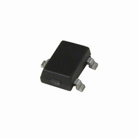
A1212LLHLT-T Allegro Microsystems Inc, A1212LLHLT-T Datasheet - Page 9

A1212LLHLT-T
Manufacturer Part Number
A1212LLHLT-T
Description
IC LATCH HALL EFFECT SOT23W
Manufacturer
Allegro Microsystems Inc
Type
Bipolar Latchr
Datasheet
1.A1214LUA-T.pdf
(13 pages)
Specifications of A1212LLHLT-T
Sensing Range
175G Trip, -175G Release
Voltage - Supply
3.8 V ~ 24 V
Current - Supply
7.5mA
Current - Output (max)
25mA
Output Type
Digital, Open Drain
Operating Temperature
-40°C ~ 150°C
Package / Case
SOT-23W
Operate Point Typ
175G
Termination Type
SMD
No. Of Pins
3
Hall Effect Type
Latching
Supply Voltage Min
3.8V
Operating Temperature Max
150°C
Peak Reflow Compatible (260 C)
Yes
Supply Voltage
24V
Filter Terminals
SMD
Rohs Compliant
Yes
Leaded Process Compatible
Yes
Operating Temperature Min
-40°C
Output Current
20mA
Lead Free Status / RoHS Status
Lead free / RoHS Compliant
Features
-
Lead Free Status / RoHS Status
Lead free / RoHS Compliant, Lead free / RoHS Compliant
Other names
620-1017-2
A1210, A1211,
A1212, A1213,
and
OPERATION
The output of these devices switches low (turns on) when a
magnetic field perpendicular to the Hall element exceeds the
operate point threshold, B
of sinking 25 mA and the output voltage is V
that the device latches; that is, a south pole of sufficient strength
towards the branded surface of the device turns the device on,
and the device remains on with removal of the south pole. When
the magnetic field is reduced below the release point, B
the device output goes high (turns off). The difference in the
magnetic operate and release points is the hysteresis, B
the device. This built-in hysteresis allows clean switching of the
output, even in the presence of external mechanical vibration and
electrical noise.
Powering-on the device in the hysteresis range, less than B
and higher than B
correct state is attained after the first excursion beyond B
B
CONTINUOUS-TIME BENEFITS
Continuous-time devices, such as the A121x family, offer the
fastest available power-on settling time and frequency response.
Figure 1. Switching Behavior of Latches. On the horizontal axis, the B+ direction indicates increasing south polarity magnetic field strength, and the
B– direction indicates decreasing south polarity field strength (including the case of increasing north polarity). This behavior can be exhibited when
using a circuit such as that shown in Panel B.
RP
.
A1214
V+
RP
0
, allows an indeterminate output state. The
B–
OP
. After turn-on, the output is capable
(A)
B
0
HYS
OUT(SAT)
B+
V
V
CC
OUT(SAT)
Functional Description
. Notice
hys
RP
OP
, of
,
OP
or
Due to offsets generated during the IC packaging process,
continuous-time devices typically require programming after
packaging to tighten magnetic parameter distributions. In con-
trast, chopper-stabilized switches employ an offset cancellation
technique on the chip that eliminates these offsets without the
need for after-packaging programming. The tradeoff is a longer
settling time and reduced frequency response as a result of the
chopper-stabilization offset cancellation algorithm.
The choice between continuous-time and chopper-stabilized
designs is solely determined by the application. Battery manage-
ment is an example where continuous-time is often required. In
these applications, V
in order to conserve power (refer to figure 2). The duty cycle
is controlled by the power-on time, t
continuous-time devices have the shorter power-on time, they
are the clear choice for such applications.
For more information on the chopper stabilization technique,
refer to Technical Paper STP 97-10, Monolithic Magnetic Hall
Sensing Using Dynamic Quadrature Offset Cancellation and
Technical Paper STP 99-1, Chopper-Stabilized Amplifiers with a
Track-and-Hold Signal Demodulator.
Continuous-Time Latch Family
V
S
CC
is chopped with a very small duty cycle
115 Northeast Cutoff
1.508.853.5000; www.allegromicro.com
Allegro MicroSystems, Inc.
Worcester, Massachusetts 01615-0036 U.S.A.
A121x
(B)
VCC
GND
VOUT
PO
, of the device. Because
R
L
Output
9


