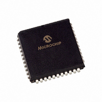
PIC18F448-I/L Microchip Technology, PIC18F448-I/L Datasheet - Page 18

PIC18F448-I/L
Manufacturer Part Number
PIC18F448-I/L
Description
IC,MICROCONTROLLER,8-BIT,PIC CPU,CMOS,LDCC,44PIN,PLASTIC
Manufacturer
Microchip Technology
Series
PIC® 18Fr
Datasheets
1.PIC18LF242-ISO.pdf
(36 pages)
2.PIC18F248-ISO.pdf
(402 pages)
3.PIC18F248-ISO.pdf
(8 pages)
Specifications of PIC18F448-I/L
Rohs Compliant
YES
Core Processor
PIC
Core Size
8-Bit
Speed
40MHz
Connectivity
CAN, I²C, SPI, UART/USART
Peripherals
Brown-out Detect/Reset, LVD, POR, PWM, WDT
Number Of I /o
33
Program Memory Size
16KB (8K x 16)
Program Memory Type
FLASH
Eeprom Size
256 x 8
Ram Size
768 x 8
Voltage - Supply (vcc/vdd)
4.2 V ~ 5.5 V
Data Converters
A/D 8x10b
Oscillator Type
External
Operating Temperature
-40°C ~ 85°C
Package / Case
44-PLCC
Processor Series
PIC18F
Core
PIC
Data Bus Width
8 bit
Data Ram Size
768 B
Interface Type
SPI, I2C, USART
Maximum Clock Frequency
40 MHz
Number Of Programmable I/os
33
Number Of Timers
4
Operating Supply Voltage
2 V to 5.5 V
Maximum Operating Temperature
+ 85 C
Mounting Style
SMD/SMT
3rd Party Development Tools
52715-96, 52716-328, 52717-734, 52712-325, EWPIC18
Development Tools By Supplier
PG164130, DV164035, DV244005, DV164005, PG164120, ICE2000, DV164136, DM163011
Minimum Operating Temperature
- 40 C
On-chip Adc
10 bit, 8 Channel
Lead Free Status / RoHS Status
Contains lead / RoHS non-compliant
For Use With
AC164309 - MODULE SKT FOR PM3 44PLCC444-1001 - DEMO BOARD FOR PICMICRO MCUDVA16XL441 - ADAPTER DEVICE ICE 44PLCCDV007003 - PROGRAMMER UNIVERSAL PROMATE II
Lead Free Status / Rohs Status
Details
Other names
PIC18F448I/L
Available stocks
Company
Part Number
Manufacturer
Quantity
Price
Company:
Part Number:
PIC18F448-I/L
Manufacturer:
Microchip Technology
Quantity:
10 000
PIC18FXX2/XX8
3.4
The ID locations are programmed much like the code
memory, except that multi-panel writes must be
disabled. The single panel that will be written will auto-
matically be enabled, based on the value of the Table
Pointer. The ID registers are mapped in addresses
200000h through 200007h. These locations read out
normally, even after code protection.
TABLE 3-7:
In order to modify the ID locations, refer to the
methodology described in Section 3.2.2, “Modifying
Code Memory”. As with code memory, the ID locations
must be erased before modified.
DS39576C-page 18
Step 1: Direct access to config memory.
Step 2: Configure device for single panel writes.
Step 3: Direct access to code memory.
Step 4: Load write buffer. Panel will be automatically determined by address.
Command
0000
0000
0000
0000
0000
0000
0000
0000
1100
0000
0000
0000
0000
0000
0000
0000
0000
1101
1101
1101
1111
0000
4-Bit
ID Location Programming
8E A6
8C A6
0E 3C
6E F8
0E 00
6E F7
0E 06
6E F6
00 00
8E A6
9C A6
0E 20
6E F8
0E 00
6E F7
0E 00
6E F6
<LSB><MSB>
<LSB><MSB>
<LSB><MSB>
<LSB><MSB>
00 00
WRITE ID SEQUENCE
Data Payload
BSF
BSF
MOVLW 3Ch
MOVWF TBLPTRU
MOVLW 00h
MOVWF TBLPTRH
MOVLW 06h
MOVWF TBLPTRL
Write 00h to 3C0006h to enable single panel writes.
BSF
BCF
MOVLW 20h
MOVWF TBLPTRU
MOVLW 00h
MOVWF TBLPTRH
MOVLW 00h
MOVWF TBLPTRL
Write 2 bytes and post-increment address by 2
Write 2 bytes and post-increment address by 2
Write 2 bytes and post-increment address by 2
Write 2 bytes and start programming
NOP - hold SCLK high for time P9
EECON1, EEPGD
EECON1, CFGS
EECON1, EEPGD
EECON1, CFGS
Figure 3-7 demonstrates the code sequence required
to write the ID locations.
Note:
Core Instruction
For single panel programming, the user
must still fill the 8-byte data buffer for the
panel.
2010 Microchip Technology Inc.


