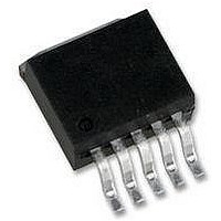
LP3966ES-ADJ National Semiconductor, LP3966ES-ADJ Datasheet - Page 6

LP3966ES-ADJ
Manufacturer Part Number
LP3966ES-ADJ
Description
Linear Voltage Regulator IC
Manufacturer
National Semiconductor
Datasheets
1.LP3966ES-ADJ.pdf
(17 pages)
2.LP3966ES-ADJ.pdf
(14 pages)
3.LP3966ES-ADJ.pdf
(14 pages)
Specifications of LP3966ES-ADJ
No. Of Pins
5
Output Current
3A
Peak Reflow Compatible (260 C)
No
Termination Type
SMD
Current Rating
3000A
Output Voltage Max
5V
Leaded Process Compatible
No
Mounting Type
Through Hole
Lead Free Status / RoHS Status
Contains lead / RoHS non-compliant
Available stocks
Company
Part Number
Manufacturer
Quantity
Price
Company:
Part Number:
LP3966ES-ADJ
Manufacturer:
NS
Quantity:
1 553
Part Number:
LP3966ES-ADJ
Manufacturer:
NS/国半
Quantity:
20 000
www.national.com
Electrical Characteristics
LP3963/LP3966
SHORT CIRCUIT PROTECTION
OVER TEMPERATURE PROTECTION
SHUTDOWN INPUT
Absolute Maximum Ratings
If Military/Aerospace specified devices are required,
please contact the National Semiconductor Sales Office/
Distributors for availability and specifications.
Storage Temperature Range
Lead Temperature
ESD Rating (Note 3)
Power Dissipation (Note 2)
Input Supply Voltage (Survival)
Shutdown Input Voltage (Survival)
Output Voltage (Survival), (Note
6), (Note 7)
Limits in standard typeface are for T
range. Unless otherwise specified: V
Symbol
Tsh(h)
Tsh(t)
T
(Soldering, 5 sec.)
I
V
V
V
T
I
I
O(PK)
V
GND
GND
V
V
I
I
dOFF
I
V
OUT
dON
V
SDT
OUT
IN
SC
SD
TH
O
T
O
OL
-
/
Output Voltage
Tolerance
(Note 8)
Output Voltage Line
Regulation (Note 8)
Output Voltage Load
Regulation
(Note 8)
Dropout Voltage
(Note 10)
Ground Pin Current In
Normal Operation
Mode
Ground Pin Current In
Shutdown Mode
(Note 11)
Peak Output Current
Short Circuit Current
Shutdown Threshold
Thermal Shutdown
Hysteresis
Shutdown Threshold
Turn-off delay
Turn-on delay
SD Input Current
Threshold
Threshold Hysteresis
Parameter
J
IN
= 25˚C, and limits in boldface type apply over the full operating temperature
= V
−0.3V to V
−65˚C to +150˚C
Internally Limited
O(NOM)
−0.3V to +7.5V
−0.3V to +7.5V
V
7.0V
10 mA
V
7.0V,
10 mA
I
I
I
I
V
(Note 2)
Output = High
Output = Low
I
I
V
(Note 9)
(Note 9)
(Note 1)
L
L
L
L
L
L
OUT
OUT
SD
SD
= 300 mA
= 3A
= 300 mA
= 3A
= 3A
= 3A
+ 1.5V, I
= V
IN
+1.5V
+1.5V
Conditions
0.2V
260˚C
<
<
+0.3V
IN
2 kV
I
I
L
L
<
<
<
<
L
3A
3A
V
V
= 10 mA, C
6
IN
IN
<
<
I
Maximum Voltage for ERROR Pin
Maximum Voltage for SENSE Pin
Operating Ratings
OUT
Input Supply Voltage (Operating)
Shutdown Input Voltage
(Operating)
Maximum Operating Current
(DC)
Operating Junction Temp. Range
(Survival)
OUT
Typ(Note
=10µF, V
0.02
0.06
0.06
0.01
800
165
V
4.5
5.5
80
15
10
20
25
10
4)
6
0
5
0
1
5
IN
SD
= V
V
LP3963/6 (Note 5)
IN
Min
-1.5
-3.0
3.5
IN
–0.3
4
5
2
-0.3V.
Short Circuit Protected
1000
1200
Max
+1.5
+3.0
−0.3V to V
100
120
0.2
10
14
15
25
75
16
−40˚C to +125˚C
9
8
2.5V to 7.0V
V
OUT
IN
V
+0.3V
IN
Units
mV
mA
+0.3V
+0.3V
µA
nA
˚C
˚C
µs
µs
%
%
%
%
%
A
A
V
3A


