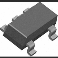
LP2981AIM5-2.5 National Semiconductor, LP2981AIM5-2.5 Datasheet - Page 5

LP2981AIM5-2.5
Manufacturer Part Number
LP2981AIM5-2.5
Description
Linear Voltage Regulator IC
Manufacturer
National Semiconductor
Datasheets
1.LP2981IM5-5.0.pdf
(16 pages)
2.LP2981IM5-5.0.pdf
(16 pages)
3.LP2981IM5-5.0.pdf
(16 pages)
Specifications of LP2981AIM5-2.5
Primary Input Voltage
16V
Dropout Voltage Vdo
200mV
No. Of Pins
5
Output Current
100mA
Operating Temperature Range
-40°C To +125°C
Termination Type
SMD
Mounting Type
Surface Mount
Lead Free Status / RoHS Status
Contains lead / RoHS non-compliant
Available stocks
Company
Part Number
Manufacturer
Quantity
Price
Part Number:
LP2981AIM5-2.5/NOPB
Manufacturer:
TI/德州仪器
Quantity:
20 000
Electrical Characteristics
Note 1: Absolute maximum ratings indicate limits beyond which damage to the component may occur. Electrical specifications do not apply when operating the de-
vice outside of its rated operating conditions.
Note 2: The ESD rating of pins 3 and 4 is 1 kV.
Note 3: The maximum allowable power dissipation is a function of the maximum junction temperature, T
the ambient temperature, T
The value of
cessive die temperature, and the regulator will go into thermal shutdown.
Note 4: If used in a dual-supply system where the regulator load is returned to a negative supply, the LP2981 output must be diode-clamped to ground.
Note 5: The output PNP structure contains a diode between the V
will turn on this diode (see Application Hints).
Note 6: Limits are 100% production tested at 25˚C. Limits over the operating temperature range are guaranteed through correlation using Statistical Quality Control
(SQC) methods. The limits are used to calculate National’s Average Outgoing Quality Level (AOQL).
Note 7: Dropout voltage is defined as the input to output differential at which the output voltage drops 100 mV below the value measured with a 1V differential.
Note 8: The ON/OFF inputs must be properly driven to prevent misoperation. For details, refer to Application Hints.
Note 9: See Typical Performance Characteristics curves.
Basic Application Circuit
additional stability margin (see Application Hints).
*
**
***
ON/OFF input must be actively terminated. Tie to V
Minimum Output Capacitance is shown to insure stability over full load current range. More capacitance provides superior dynamic performance and
Do not make connections to this pin.
JA
for the SOT-23 package is 220˚C/W and the micro SMD package is 320˚C/W. Exceeding the maximum allowable power dissipation will cause ex-
A
. The maximum allowable power dissipation at any ambient temperature is calculated using:
IN
(Continued)
if this function is not to be used.
IN
and V
OUT
terminals that is normally reverse-biased. Reversing the polarity from V
5
J(MAX)
, the junction-to-ambient thermal resistance,
DS012506-4
www.national.com
IN
to V
JA
, and
OUT


