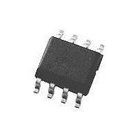
LP2975IMM-5.0 National Semiconductor, LP2975IMM-5.0 Datasheet - Page 15

LP2975IMM-5.0
Manufacturer Part Number
LP2975IMM-5.0
Description
Driver IC
Manufacturer
National Semiconductor
Datasheets
1.LP2975IMM-5.0.pdf
(20 pages)
2.LP2975IMM-5.0.pdf
(19 pages)
3.LP2975IMM-5.0.pdf
(19 pages)
Specifications of LP2975IMM-5.0
Device Type
LDO
Driver Case Style
SOIC
No. Of Pins
8
Mounting Type
Surface Mount
Voltage Regulator Type
LDO Linear
Supply Voltage Min
1.8V
Peak Reflow Compatible (260 C)
No
Output Voltage
5V
Output Voltage Max
5V
Lead Free Status / RoHS Status
Contains lead / RoHS non-compliant
Available stocks
Company
Part Number
Manufacturer
Quantity
Price
Company:
Part Number:
LP2975IMM-5.0
Manufacturer:
MICROCHIP
Quantity:
2 000
Company:
Part Number:
LP2975IMM-5.0
Manufacturer:
NS
Quantity:
8 141
Company:
Part Number:
LP2975IMM-5.0
Manufacturer:
NS
Quantity:
572
Part Number:
LP2975IMM-5.0
Manufacturer:
NS/国半
Quantity:
20 000
Part Number:
LP2975IMM-5.0/NOPB
Manufacturer:
NS/国半
Quantity:
20 000
Application Hints
G
G
sheet specifies forward transconductance (G
value of drain current (defined as I
desired value of load current (defined as I
Where:
R
ESR is the equivalent series resistance of the output
capacitor.
The term R
It can be seen from these equations that C
To get the worst-case (maximum) value for C
maximum value of load current, which also means the mini-
mum value of load resistance R
most cases, the ESR is the dominant term which determines
the value of R
Gate Capacitance Pole Frequency (f
The pole frequency resulting from the Gate capacitance
C
Where:
R
drives the Gate of the FET. It is important to note that R
a function of input supply voltage (see graph GATE PIN
OUTPUT IMPEDANCE).As shown, the minimum value of
R
Using the equation for f
showing how f
(see graph f
@
L
EFF
O
O
GD
m
V
is the load resistance.
is the output impedance of the LP2975 Gate pin which
is about 550Ω
IN
is the transconductance of the FET. The FET data
is the Gate-to-Drain capacitance, which is equal to:
is defined as f
= 3V.
L
pg
/ / ESR is defined as:
L
pg
Gate Pin Output Impedance
vs. C
/ / ESR.
(R
varies with C
f
pg
@
G
L
C
pg
EFF
m
. 0.16 / (R
V
x ESR) / (R
GS
IN
and can be approximated from:
= G
):
C
pg
= 24V, increasing to about 1.55 kΩ
= C
GD
, a family of curves are provided
fs
ISS
= C
x (I
EFF
(Continued)
L
− C
L
RSS
O
. It should be noted that in
L
/ I
x C
+ ESR)
for several values of R
RSS
D
D
)
1/2
EFF
). To find Gm at the
pg
L
)
)
EFF
), use the formula:
10003420
varies with R
EFF
fs
) at some
, use the
O
L
is
O
.
15
As can be seen in the graph, values of C
500 pF–2500 pF range produce values for f
40 kHz and 700 kHz. To determine what effect f
on stability, the bandwidth of the regulator loop must be
calculated (see next section CROSSOVER FREQUENCY
AND PHASE MARGIN).
Crossover Frequency and Phase Margin
The term f
the regulator loop (which is the frequency where the gain
curve crosses the 0 dB axis). The importance of this fre-
quency is that it is the point where the loop gain goes below
unity, which marks the usable bandwidth of the regulator
loop.
It is the phase margin (or lack of it) at f
whether the regulator is stable. Phase margin is defined as
the total phase shift subtracted from 180˚. In general, a
stable loop requires at least 20˚-30˚ of phase margin at f
f
have been previously defined):
This equation assumes that no C
If the frequency of the Gate capacitance pole f
calculated (previous section), the amount of added phase
shift may now be determined. As shown in the graph below
(see graph PHASE SHIFT DUE TO f
added phase shift increases as f
The amount of phase shift due to f
oscillation takes place depends on how much added phase
shift is present as a result of the C
section OUTPUT CAPACITOR).
c
can be approximated by the following equation (all terms
c
will be used to define the crossover frequency of
f
pg
vs. C
EFF
pg
F
is used and f
pg
approaches f
OUT
that can occur before
pg
pole (see previous
c
), the amount of
10003423
that determines
10003421
pg
pg
pg
www.national.com
EFF
pg
c
.
/f
has been
will have
between
c
in the
>
1.
c
.


