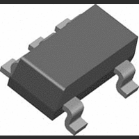
LMC7111BIM5 National Semiconductor, LMC7111BIM5 Datasheet - Page 15

LMC7111BIM5
Manufacturer Part Number
LMC7111BIM5
Description
Operational Amplifier (Op-Amp) IC
Manufacturer
National Semiconductor
Specifications of LMC7111BIM5
No. Of Amplifiers
1
No. Of Pins
5
Peak Reflow Compatible (260 C)
No
Leaded Process Compatible
No
Mounting Type
Surface Mount
Package / Case
5-SOT-23
Lead Free Status / RoHS Status
Contains lead / RoHS non-compliant
Available stocks
Company
Part Number
Manufacturer
Quantity
Price
Company:
Part Number:
LMC7111BIM5
Manufacturer:
NSC
Quantity:
100 000
Company:
Part Number:
LMC7111BIM5
Manufacturer:
NS
Quantity:
5 085
Part Number:
LMC7111BIM5
Manufacturer:
NSC
Quantity:
20 000
Company:
Part Number:
LMC7111BIM5/NOPB
Manufacturer:
AD
Quantity:
4 223
Company:
Part Number:
LMC7111BIM5/NOPB
Manufacturer:
Texas Instruments
Quantity:
1
Part Number:
LMC7111BIM5/NOPB
Manufacturer:
NS/国半
Quantity:
20 000
Company:
Part Number:
LMC7111BIM5X
Manufacturer:
NS
Quantity:
5 321
Company:
Part Number:
LMC7111BIM5X
Manufacturer:
NS
Quantity:
1 792
Part Number:
LMC7111BIM5X
Manufacturer:
TI/德州仪器
Quantity:
20 000
Company:
Part Number:
LMC7111BIM5X/NOPB
Manufacturer:
Texas Instruments
Quantity:
1
Part Number:
LMC7111BIM5X/NOPB
Manufacturer:
TI/德州仪器
Quantity:
20 000
Application Information
1.0 BENEFITS OF THE LMC7111
TINY AMP
Size
The small footprint of the SOT 23-5 packaged Tiny amp,
(0.120 x 0.118 inches, 3.05 x 3.00 mm) saves space on
printed circuit boards, and enable the design of smaller
electronic products. Because they are easier to carry, many
customers prefer smaller and lighter products.
Height
The height (0.056 inches, 1.43 mm) of the Tiny amp makes
it possible to use it in PCMCIA type III cards.
Signal Integrity
Signals can pick up noise between the signal source and the
amplifier. By using a physically smaller amplifier package,
the Tiny amp can be placed closer to the signal source,
reducing noise pickup and increasing signal integrity. The
Tiny amp can also be placed next to the signal destination,
such as a buffer for the reference of an analog to digital
converter.
Simplified Board Layout
The Tiny amp can simplify board layout in several ways.
First, by placing an amp where amps are needed, instead of
routing signals to a dual or quad device, long pc traces may
be avoided.
By using multiple Tiny amps instead of duals or quads,
complex signal routing and possibly crosstalk can be re-
duced.
DIPs available for prototyping
LMC7111 amplifiers packaged in conventional 8-pin dip
packages can be used for prototyping and evaluation without
the need to use surface mounting in early project stages.
Low Supply Current
The typical 25 µA supply current of the LMC7111 extends
battery life in portable applications, and may allow the reduc-
tion of the size of batteries in some applications.
Wide Voltage Range
The LMC7111 is characterized at 2.7V, 3V, 3.3V, 5V and 10V.
Performance data is provided at these popular voltages. This
wide voltage range makes the LMC7111 a good choice for
devices where the voltage may vary over the life of the
batteries.
2.0 INPUT COMMON MODE
VOLTAGE RANGE
The LMC7111 does not exhibit phase inversion when an
input voltage exceeds the negative supply voltage.
The absolute maximum input voltage is 300 mV beyond
either rail at room temperature. Voltages greatly exceeding
this maximum rating can cause excessive current to flow in
or out of the input pins, adversely affecting reliability.
Applications that exceed this rating must externally limit the
maximum input current to
shown in Figure 1.
±
5 mA with an input resistor as
15
3.0 CAPACITIVE LOAD TOLERANCE
The LMC7111 can typically directly drive a 300 pF load with
V
follower is the most sensitive configuration. Direct capacitive
loading reduces the phase margin of op-amps. The combi-
nation of the op-amp’s output impedance and the capacitive
load induces phase lag. This results in either an under-
damped pulse response or oscillation.
Capacitive load compensation can be accomplished using
resistive isolation as shown in Figure 2. This simple tech-
nique is useful for isolating the capacitive input of multiplex-
ers and A/D converters.
4.0 COMPENSATING FOR INPUT CAPACITANCE WHEN
USING LARGE VALUE FEEDBACK RESISTORS
When using very large value feedback resistors, (usually
input capacitance due to transducers, photodiodes, and cir-
cuit board parasitics to reduce phase margins.
The effect of input capacitance can be compensated for by
adding a feedback capacitor. The feedback capacitor (as in
Figure 3), C
or
which typically provides significant overcompensation.
Printed circuit board stray capacitance may be larger or
smaller than that of a breadboard, so the actual optimum
value for C
checked on the actual circuit. (Refer to the LMC660 quad
CMOS amplifier data sheet for a more detailed discussion.)
>
S
500 kΩ) the large feed back resistance can react with the
= 10V at unity gain without oscillating. The unity gain
FIGURE 1. R
Voltages Exceeding the Supply Voltage
F
f
is first estimated by:
may be different. The values of C
FIGURE 2. Resistive Isolation
of a 330 pF Capacitive Load
I
Input Current Protection for
R
1
C
IN
≤ R
2
C
f
01235212
01235214
F
www.national.com
should be


