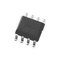
LM3485MM National Semiconductor, LM3485MM Datasheet - Page 10

LM3485MM
Manufacturer Part Number
LM3485MM
Description
Pulse Width Modulation (PWM) Controller IC
Manufacturer
National Semiconductor
Specifications of LM3485MM
Input Voltage Primary Min
4.5V
Mounting Type
Surface Mount
Topology
Buck (Step Down)
Control Mode
Hysteretic
Duty Cycle Max
100%
Input Voltage Primary Max
35V
Lead Free Status / RoHS Status
Contains lead / RoHS non-compliant
Available stocks
Company
Part Number
Manufacturer
Quantity
Price
Company:
Part Number:
LM3485MM
Manufacturer:
TI
Quantity:
6 020
Part Number:
LM3485MM
Manufacturer:
NS/国半
Quantity:
20 000
Company:
Part Number:
LM3485MM/NOPB
Manufacturer:
TI
Quantity:
5 600
Part Number:
LM3485MM/NOPB
Manufacturer:
NS/国半
Quantity:
20 000
Part Number:
LM3485MM/NS
Manufacturer:
NS/国半
Quantity:
20 000
Company:
Part Number:
LM3485MMX
Manufacturer:
NS
Quantity:
5 321
Part Number:
LM3485MMX
Manufacturer:
TI/德州仪器
Quantity:
20 000
www.national.com
Functional Description
The minimum output voltage ripple (V
lated in the same way.
For example, with V
Operating frequency (F) is determined by knowing the input
voltage, output voltage, inductor, V
Series Resistance) of output capacitor, and the delay. It can
be approximately calculated using the formula:
where:
and the PFET delay time. The propagation delay is 90ns
The operating frequency and output ripple voltage can also
be significantly influenced by the speed up capacitor (Cff).
Cff is connected in parallel with the high side feedback
resistor, R1. The location of this capacitor is similar to where
a feed forward capacitor would be located in a PWM control
scheme. However it’s effect on hysteretic operation is much
different. The output ripple causes a current to be sourced or
sunk through this capacitor. This current is essentially a
square wave. Since the input to the feedback pin, FB, is a
high impedance node, the current flows through R2. The end
result is a reduction in output ripple and an increase in
operating frequency. When adding Cff, calculate the formula
above with
operating frequency and the value of R2. A good starting
point is 470pF ceramic at 100kHz decreasing linearly with
increased operating frequency. Also note that as the output
voltage is programmed below 2.5V, the effect of Cff will
decrease significantly.
delay: It includes the LM3485 propagation delay time
typically. (See the Propagation Delay curve below.)
: ( R1 + R2 ) / R2
V
OUT_PP
V
OUT_PP
FIGURE 2. Propagation Delay
= 1. The value of Cff depend on the desired
= 0.01* ( 33K + 20K ) / 20K = 0.0266V
OUT
= V
set to 3.3V, V
HYST
( R1 + R2 ) / R2
HYST
OUT_PP
OUT_PP
(Continued)
, ESR (Equivalent
) can be calcu-
is 26.6mV
20034614
10
CURRENT LIMIT OPERATION
The LM3485 has a cycle-by-cycle current limit. Current limit
is sensed across the V
tional sense resistor. When current limit is activated, the
LM3485 turns off the external PFET for a period of 9µs(typi-
cal). The current limit is adjusted by an external resistor,
R
The current limit circuit is composed of the ISENSE com-
parator and the one-shot pulse generator. The positive input
of the ISENSE comparator is the ADJ pin. An internal 5.5µA
current sink creates a voltage across the external R
resistor. This voltage is compared to the voltage across the
PFET or sense resistor. The ADJ voltage can be calculated
as follows:
Where 3.0µA is the minimum I
The negative input of the ISENSE comparator is the ISENSE
pin that should be connected to the drain of the external
PFET. The inductor current is determined by sensing the
V
The current limit is activated when the voltage at the ADJ pin
exceeds the voltage at the I
parator triggers the 9µs one shot pulse generator forcing the
driver to turn the PFET off. The driver turns the PFET back
on after 9µs. If the current has not reduced below the set
threshold, the cycle will repeat continuously.
A filter capacitor, C
3. C
tor will not be accidentally triggered. A value of 100pF to 1nF
is recommended in most applications. Higher values can be
used to create a soft-start function (See Start Up section).
The current limit comparator has approximately 100ns of
blanking time. This ensures that the PFET is fully on when
the current is sensed. However, under extreme conditions
such as cold temperature, some PFETs may not fully turn on
within the blanking time. In this case, the current limit thresh-
old must be increased. If the current limit function is used,
the on time must be greater than 100ns. Under low duty
cycle operation, the maximum operating frequency will be
limited by this minimum on time.
During current limit operation, the output voltage will drop
significantly as will operating frequency. As the load current
is reduced, the output will return to the programmed voltage.
However, there is a current limit fold back phenomenon
inherent in this current limit architecture. See Figure 4.
DS
ADJ
. It can be calculated as follows.
ADJ
.
V
ISENSE
filters unwanted noise so that the ISENSE compara-
FIGURE 3. Current Sensing by V
= V
V
ADJ
IN
ADJ
− (R
= V
, should be placed as shown in Figure
DS
DSON
IN
of the PFET or across an addi-
− (R
SENSE
* I
CL-ADJ
ADJ
IND_PEAK
* 3.0µA)
pin. The ISENSE com-
value.
) = V
IN
DS
− V
20034625
DS
ADJ


