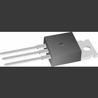
LM1084IS-5.0 National Semiconductor, LM1084IS-5.0 Datasheet - Page 9

LM1084IS-5.0
Manufacturer Part Number
LM1084IS-5.0
Description
Linear Voltage Regulator IC
Manufacturer
National Semiconductor
Datasheets
1.LM1084ISX-ADJ.pdf
(13 pages)
2.LM1084ISX-ADJ.pdf
(13 pages)
3.LM1084ISX-ADJ.pdf
(14 pages)
Specifications of LM1084IS-5.0
No. Of Pins
3
Output Current
1.5A
Termination Type
Through Hole
Mounting Type
Through Hole
Voltage Regulator Type
LDO Linear
Peak Reflow Compatible (260 C)
No
Supply Voltage
29V
Current Rating
5A
Lead Free Status / RoHS Status
Contains lead / RoHS non-compliant
Available stocks
Company
Part Number
Manufacturer
Quantity
Price
Company:
Part Number:
LM1084IS-5.0
Manufacturer:
NS
Quantity:
500
Application Note
must be added, one for case to heat-sink (θ
heatsink to ambient (θ
predicted as follows:
T
T
P
consumption is calculated as follows:
Once the devices power is determined, the maximum allow-
able (θ
θ
The LM1084 has different temperature specifications for two
different sections of the IC: the control section and the output
section. The Electrical Characteristics table shows the junc-
tion to case thermal resistances for each of these sections,
while the maximum junction temperatures (T
section is listed in the Absolute Maximum section of the
datasheet. T
T
θ
follows:
θ
θ
The required heat sink is determined by calculating its re-
quired thermal resistance (θ
JA (max)
JA (max)
JA
JA
J
J
J(max)
D
= T
is junction temperature, T
is the power consumption of the device. Device power
(max, CONTROL SECTION) = (125˚C - T
(max, OUTPUT SECTION) = (150˚C - T
A
JA (max)
is 150˚C for the output section.
+ P
should be calculated separately for each section as
= T
D
R(max)
J(max)
(θ
) is calculated as:
JC
/P
+ θ
is 125˚C for the control section, while
D
CH
HA
= T
). The junction temperature can be
+ θ
J(max)
HA (max)
HA
A
(Continued)
) = T
is ambient temperature, and
− T
A(max)
).
A
FIGURE 7. Heat sink thermal Resistance vs Area
+ P
/P
D
FIGURE 6. Power Dissipation Diagram
D
θ
CH
A(max)
JA
J(max)
A(max)
) and one for
) for each
)/P
)/P
D
D
9
Figure 6 shows the voltages and currents which are present
in the circuit.
θ
(θ
(θ
TROL SECTION) + θ
(θ
SECTION) + θ
If thermal compound is used, θ
C/W. If the case is soldered to the heat sink, then a θ
be estimated as 0 C/W.
After, θ
lower of the two θ
ate heat sink.
If PC board copper is going to be used as a heat sink, then
Figure 7 can be used to determine the appropriate area
(size) of copper foil required.
HA (max)
HA (max)
HA (max)
HA (max)
I
P
IN
D
HA (max)
= I
= (V
= θ
) should also be calculated twice as follows:
) = θ
) = θ
L
10094664
+ I
IN
JA (max)
JA
−V
JA
G
CH
(max, OUTPUT SECTION) - (θ
is calculated for each section, choose the
OUT
(max, CONTROL SECTION) - (θ
)
10094616
HA (max)
− (θ
) I
CH
L
)
+ V
JC
values to determine the appropri-
+ θ
IN
I
G
CH
CH
)
can be estimated at 0.2
JC
www.national.com
(OUTPUT
JC
CH
(CON-
can


