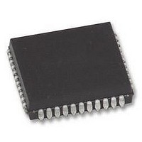
P89V51RB2FA NXP Semiconductors, P89V51RB2FA Datasheet - Page 43

P89V51RB2FA
Manufacturer Part Number
P89V51RB2FA
Description
MCU 8BIT 80C51 16K FLASH, PLCC44
Manufacturer
NXP Semiconductors
Datasheet
1.P89V51RC2FBC557.pdf
(80 pages)
Specifications of P89V51RB2FA
Controller Family/series
(8051) 8052
Core Size
8bit
No. Of I/o's
32
Program Memory Size
16KB
Ram Memory Size
1KB
Cpu Speed
40MHz
Oscillator Type
External Only
No. Of Timers
4
No. Of Pwm
RoHS Compliant
Available stocks
Company
Part Number
Manufacturer
Quantity
Price
Company:
Part Number:
P89V51RB2FA
Manufacturer:
NXP
Quantity:
1 000
Company:
Part Number:
P89V51RB2FA
Manufacturer:
NXP
Quantity:
2 000
Part Number:
P89V51RB2FA
Manufacturer:
NXP/恩智浦
Quantity:
20 000
Part Number:
P89V51RB2FA (FLA
Manufacturer:
NXP/恩智浦
Quantity:
20 000
Company:
Part Number:
P89V51RB2FA,529
Manufacturer:
NXP Semiconductors
Quantity:
10 000
Company:
Part Number:
P89V51RB2FAЈ¬529
Manufacturer:
NXP
Quantity:
150
NXP Semiconductors
P89V51RB2_RC2_RD2_5
Product data sheet
Fig 17. SPI master-slave interconnection
CLOCK GENERATOR
SPI
clock output and input for the master and slave modes, respectively. The SPI clock
generator will start following a write to the master devices SPI data register. The written
data is then shifted out of the MOSI pin on the master device into the MOSI pin of the
slave device. Following a complete transmission of one byte of data, the SPI clock
generator is stopped and the SPIF flag is set. An SPI interrupt request will be generated if
the SPI Interrupt Enable bit (SPIE) and the Serial Port Interrupt Enable bit (ES) are both
set.
An external master drives the Slave Select input pin, SS/P1[4], low to select the SPI
module as a slave. If SS/P1[4] has not been driven low, then the slave SPI unit is not
active and the MOSI/P1[5] port can also be used as an input port pin.
CPHA and CPOL control the phase and polarity of the SPI clock.
show the four possible combinations of these two bits.
Table 28.
Bit addressable; Reset source(s): any reset; Reset value: 0000 0000B
Table 29.
Bit
7
6
5
4
3
Bit
Symbol
8-BIT SHIFT REGISTER
MSB master LSB
SPCR - SPI control register (address D5H) bit allocation
SPCR - SPI control register (address D5H) bit description
Symbol
SPIE
SPE
DORD
MSTR
CPOL
SPIE
7
Rev. 05 — 12 November 2009
SPE
6
Description
If both SPIE and ES are set to one, SPI interrupts are enabled.
SPI enable bit. When set enables SPI.
Data transmission order. 0 = MSB first; 1 = LSB first in data
transmission.
Master/slave select. 1 = master mode, 0 = slave mode.
Clock polarity. 1 = SPICLK is high when idle (active LOW),
0 = SPICLK is low when idle (active HIGH).
MISO
MOSI
SPICLK
SS
V
DD
DORD
5
SPICLK
V
MISO
MOSI
SS
MSTR
SS
P89V51RB2/RC2/RD2
4
8-bit microcontrollers with 80C51 core
CPOL
3
8-BIT SHIFT REGISTER
MSB slave LSB
CPHA
2
Figure 18
© NXP B.V. 2009. All rights reserved.
SPR1
002aaa528
1
and
Figure 19
SPR0
43 of 80
0


