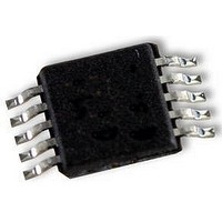
AD8592ARMZ Analog Devices Inc, AD8592ARMZ Datasheet - Page 9

AD8592ARMZ
Manufacturer Part Number
AD8592ARMZ
Description
OP AMP, +SHUTDOWN RRI/O, SMD, 8592
Manufacturer
Analog Devices Inc
Datasheet
1.AD8592ARMZ.pdf
(15 pages)
Specifications of AD8592ARMZ
Op Amp Type
Low Input Bias
No. Of Amplifiers
2
Bandwidth
2.2MHz
Slew Rate
5V/µs
Supply Voltage Range
2.5V To 6V
Amplifier Case Style
MSOP
No. Of Pins
10
Operating Temperature Range
-40°C To
Lead Free Status / RoHS Status
Lead free / RoHS Compliant
Available stocks
Company
Part Number
Manufacturer
Quantity
Price
Company:
Part Number:
AD8592ARMZ
Manufacturer:
Analog Devices Inc
Quantity:
31 712
Company:
Part Number:
AD8592ARMZ
Manufacturer:
AD
Quantity:
8 241
Part Number:
AD8592ARMZ
Manufacturer:
ADI/亚德诺
Quantity:
20 000
Company:
Part Number:
AD8592ARMZ-REEL
Manufacturer:
AD
Quantity:
1 538
Company:
Part Number:
AD8592ARMZ-REEL
Manufacturer:
Microsemi
Quantity:
1 538
Part Number:
AD8592ARMZ-REEL
Manufacturer:
ADI/亚德诺
Quantity:
20 000
Company:
Part Number:
AD8592ARMZ-REEL7
Manufacturer:
TOREX
Quantity:
800
In any application, the absolute maximum junction temperature
must be limited to +150 C. If this junction temperature is ex-
ceeded, the device could suffer premature failure. If the output
voltage and output current are in phase, for example, with a
purely resistive load, the power dissipated by the AD859x can
be found as:
Where
By calculating the power dissipation of the device and using the
thermal resistance value for a given package type, the maximum
allowable ambient temperature for an application can be found
using Equation 3.
Capacitive Loading
The AD859x exhibits excellent capacitive load driving capabilities
and can drive up to 10 nF directly. Although the device is stable
with large capacitive loads, there is a decrease in amplifier band-
width as the capacitive load increases. Figure 31 shows a graph of
the AD8592 unity gain bandwidth under various capacitive loads.
When driving heavy capacitive loads directly from the AD859x
output, a snubber network can be used to improve transient
response. This network consists of a series R-C connected from
the amplifier’s output to ground, placing it in parallel with the
capacitive load. The configuration is shown in Figure 32. Al-
though this network will not increase the bandwidth of the am-
plifier, it will significantly reduce the amount of overshoot, as
shown in Figure 33.
REV. A
Figure 31. Unity Gain Bandwidth vs. Capacitive Load
P
Figure 32. Configuration for Snubber Network to
Compensate for Capacitive Loads
D
ISS
3.5
2.5
1.5
0.5
4
3
2
1
0
I
V
V
100mV p-p
0.01
LOAD
SY
OUT
I
= AD859x supply voltage; and
LOAD
V
= The output voltage
= AD859x output load current
IN
0.1
V
SY
AD8592
CAPACITIVE LOAD – nF
+5V
–
V
OUT
1
R
5
C
1 F
S
S
10
C
47nF
L
V
R
T
A
S
L
=
= 1k
= +25 C
V
OUT
2.5V
100
(4)
–9–
The optimum values for the snubber network should be determined
empirically based on the size of the capacitive load. Table I shows a
few sample snubber network values for a given load capacitance.
Load Capacitance
0.47 nF
4.7 nF
47 nF
A PC-98 Compliant Headphone/Speaker Amplifier
Because of its high output current performance and shutdown
feature, the AD8592 makes an excellent amplifier for driving an
audio output jack in a computer application. Figure 34 shows
how the AD8592 can be interfaced with an AC97 codec to drive
headphones or speakers.
Figure 34. A PC-98 Compliant Headphone/Line Out Amplifier
When headphones are plugged into the jack, the normalizing con-
tacts disconnect from the audio contacts. This allows the voltage to
the AD8592 shutdown pins to be pulled up to +5 V, activating the
amplifiers. With no plug in the output jack, the shutdown voltage is
pulled to 100 mV through the R1 and R3 + R5 voltage divider.
This powers the AD8592 down when it is not needed, saving
current from the power supply or battery.
(C
Figure 33. Snubber Network Reduces Overshoot and
Ringing Caused from Driving Heavy Capacitive Loads
L
Table I. Snubber Networks for Large Capacitive Loads
)
NOTE: ADDITIONAL PINS
OMITTED FOR CLARITY
AD1881
(AC97)
RIGHT
LEFT
47nF LOAD
IN CIRCUIT
SNUBBER
V
V
OUT
V
OUT
DD
DD
SS
ONLY
28
35
36
+5V
100
0%
90
10
AD8591/AD8592/AD8594
2
3
7
8
5
6
U1-A
U1-B
50mV
50mV
+5V
10
4
U1 = AD8592
100k
9
Snubber Network
(R
300 , 0.1 F
30 , 1 F
5 , 1 F
1
R1
S
+5V
, C
100 F
100 F
S
)
C1
C2
2k
2k
R2
R3
10 s
20
20
R4
R5
NC


