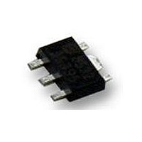
XC6214P152PR Torex Semiconductor Ltd, XC6214P152PR Datasheet

XC6214P152PR
Specifications of XC6214P152PR
Available stocks
Related parts for XC6214P152PR
XC6214P152PR Summary of contents
Page 1
XC6214 Series 500mA Output Current, High Speed LDO Regulators, Thermal Shutdown Function, Ceramic Capacitor Compatible ■GENERAL DESCRIPTION The XC6214 series are highly precise, low noise, high current, positive voltage, low dropout voltage regulators. They are fabricated using CMOS process. The ...
Page 2
XC6214 Series ■PIN CONFIGURATION OUT SOT-89 (TOP VIEW) ■PIN ASSIGNMENT PIN NUMBER SOT-89 TO-252 ■PRODUCT CLASSIFICATION ●Ordering Information (*1) XC6214P①②③④⑤-⑥ DESIGNATOR DESCRIPTION Output Voltage ...
Page 3
DIAGRAM V IN Voltage Reference * Diodes inside the circuit are ESD protection diodes and parasitic diodes. ■ABSOLUTE MAXIMUM RATINGS PARAMETER Input Voltage Output Current * Output Voltage SOT-89 Power Dissipation TO-252 Operating Temperature Range Storage Temperature Range * ...
Page 4
XC6214 Series ■ELECTRICAL CHARACTERISTICS ●XC6214P122 PARAMETER SYMBOL Output Voltage V OUT(E) Maximum Output Current I OUT Load Regulation △V Dropout Voltage (*2) Vdif Supply Current I SS △V Line Regulation △V IN ・V Input Voltage V Output Voltage △V △Topr ...
Page 5
CHARACTERISTICS (Continued) ●XC6214P182 PARAMETER SYMBOL Output Voltage V OUT(E) Maximum Output Current I max OUT Load Regulation △V OUT Dropout Voltage (*2) Vdif Supply Current I SS △V OUT Line Regulation △V IN・ Input Voltage V IN Output Voltage ...
Page 6
XC6214 Series ■ELECTRICAL CHARACTERISTICS (Continued) ●XC6214P302 PARAMETER SYMBOL Output Voltage V OUT(E) Maximum Output Current I OUT Load Regulation △V Dropout Voltage (*2) Vdif Supply Current I SS △V Line Regulation △V ・V IN Input Voltage V Output Voltage △V ...
Page 7
CIRCUITS ●Circuit ① V ●Circuit ② A CIN=1.0uF CIN=1.0μF (ceramic) (ceramic) VIN VOUT VSS CIN=1.0uF CL=1.0uF CIN=1.0μF CIN=1.0μF (ceramic) (ceramic) VIN VOUT VSS (ceramic) (ceramic) OPEN XC6214 Series 7/24 ...
Page 8
XC6214 Series ■OPERATIONAL EXPLANATION <Output Voltage Regulator Control> The voltage, divided by resistors R1 & R2, which are connected to the V voltage by the error amplifier. The P-channel MOSFET, which is connected to the V subsequent output signal. The ...
Page 9
DISSIPATION (TO-252) TO-252 Power Dissipation ● Power dissipation data for the TO-252 is shown in this page. The value of power dissipation varies with the mount board conditions. Please use this data as one of reference data taken in ...
Page 10
XC6214 Series ■TYPICAL PERFORMANCE CHARACTERISTICS (1) Output Voltage vs. Output Current XC6214P122 XC6214P122 VIN=2.25V CIN=CL=1.0μF(ceramic ) CIN=CL=1.0μF (ceramic) 1.3 1.2 1.1 1 0.9 0 100 200 Output Current : IOUT (mA) XC6214P152 XC6214P152 VIN=2.7V CIN=CL=1.0μF (ceramic) ...
Page 11
PERFORMANCE CHARACTERISTICS (Continued) (1) Output Voltage vs. Output Current (Continued) XC6214P252 XC6214P252 VIN=3.5V CIN=CL=1.0μF(ceramic ) CIN=CL=1.0μF (ceramic) 2.6 2.5 2.4 2.3 2.2 0 100 200 300 Output Current : IOUT (mA) XC6214P332 XC6214P332 ...
Page 12
XC6214 Series ■TYPICAL PERFORMANCE CHARACTERISTICS (Continued) (2) Output Voltage vs. Input Voltage (Continued) XC6214P152 XC6214P152 CIN=CL=1.0μF(ceramic ) CIN=CL=1.0μF (ceramic) 1.7 1.6 1.5 1.4 1.3 1.2 1.1 1.0 1.1 1.2 1.3 1.4 1.5 1.6 1.7 1.8 1.9 2.0 Input Voltage : ...
Page 13
PERFORMANCE CHARACTER (Continued) (2) Output Voltage vs. Input Voltage (Continued) XC6214P332 XC6214P332 CIN=CL=1.0μF(ceramic ) CIN=CL=1.0μF (ceramic) 3.5 3.3 3.1 2.9 2.7 2.5 2.8 2.9 3.0 3.1 3.2 3.3 3.4 Input Voltage : VIN (V) (3) Dropout Voltage vs. Output ...
Page 14
XC6214 Series ■TYPICAL PERFORMANCE CHARACTERISTICS (Continued) (3) Dropout Voltage vs. Output Current (Continued) XC6214P332 CIN=CL=1.0μF (ceramic) CIN=CL=1.0μF(ceramic) 1.2 1.0 0.8 0.6 0.4 0.2 0.0 0 100 200 300 Output Current : IOUT (mA) XC6214P152 CIN=1.0μF(ceramic ) CIN=1.0μF (ceramic ...
Page 15
PERFORMANCE CHARACTERISTICS (Continued) (5) Output Voltage vs. Ambient Temperature XC6214P122 XC6214P122 CIN=CL=1.0μF (ceramic) CIN=CL=1.0μF (ceramic) 1.30 1.25 1.20 1.15 1.10 -60 -40 - Ambient Temperrature:Ta (℃) XC6214P182 XC6214P182 CIN=CL=1.0μF (ceramic) CIN=CL=1.0μF (ceramic) 1.90 1.85 1.80 1.75 ...
Page 16
XC6214 Series ■TYPICAL PERFORMANCE CHARACTERISTICS (Continued) (6) Supply Current vs. Ambient Temperature (Continued) XC6214P152 XC6214P152 CIN=CL=1.0μF (ceramic) CIN=CL=1.0μF (ceramic -60 -40 - Ambient Temperrature:Ta (℃) XC6214P252 XC6214P252 CIN=CL=1.0μF (ceramic) CIN=CL=1.0μF (ceramic) 20 ...
Page 17
PERFORMANCE CHARACTERISTICS (Continued) (7) Input Transient Response XC6214P122 XC6214P122 IOUT=1mA, Ta=25℃ IOUT=1mA, Ta=25 CIN=CL=1.0μF (ceramic) CIN=CL=1.0μF(ceramic) 4 Input Voltage Output Voltage 0 -1 Time (200μs/div) Time ( 200μs/div ) XC6214P152 XC6214P152 IOUT=1mA, Ta=25℃ IOUT=1mA, Ta=25 CIN=CL=1.0μF ...
Page 18
XC6214 Series ■TYPICAL PERFORMANCE CHARACTERISTICS (Continued) (7) Input Transient Response (Continued) XC6214P252 XC6214P252 IOUT=1mA, Ta=25℃ IOUT=1mA, Ta=25 CIN=CL=1.0μF (ceramic) CIN=CL=1.0μF(ceramic Input Voltage 3 2 Output Voltage 1 0 Time ( 200μs/div ) Time (200μs/div) XC6214P332 XC6214P332 IOUT=1mA, ...
Page 19
PERFORMANCE CHARACTERISTICS (Continued) (8) Load Transient Response (Continued) XC6214P152 XC6214P152 VIN=2.5V, Ta=25℃ VIN=2.5V 、 Ta=25 CIN=CL=1.0μF (ceramic) CIN= CL=1.0μF(ceramic Output Voltage 1 0 50mA -1 Output Current 1mA -2 Time (1ms/div) XC6214P182 XC6214P182 VIN=2.8V, Ta=25℃ ...
Page 20
XC6214 Series ■TYPICAL PERFORMANCE CHARACTERISTICS (Continued) (8) Load Transient Response (Continued) XC6214P332 XC6214P332 VIN=4.3V, Ta=25℃ VIN=4.3V 、 Ta=25 CIN=CL=1.0μF (ceramic) CIN= CL=1.0μF(ceramic Output Voltage 2 50mA 1 1mA Output Current 0 Time (1ms/div) (9) Ripple Rejection ...
Page 21
PERFORMANCE CHARACTERISTICS (Continued) (9) Ripple Rejection Rate (Continued) XC6214P182 XC6214P182 VIN=2.8VDC+0.5p-pAC, IOUT=50mA VIN=2.8VDC+0.5p-pAC , IOUT=50mA CL=1.0μF (ceramic) CL=1.0uF(ceramic 0.01 0.1 Ripple Frequency : f (KHz) XC6214P252 XC6214P252 VIN=3.5VDC+0.5p-pAC, IOUT=50mA ...
Page 22
XC6214 Series ■PACKAGING INFORMATION ●SOT-89 ●TO-252 6. 55± 3± 75± 75± 75± (2 . 28) (2 . 28) 22/ ± ...
Page 23
RULE ●SOT-89, TO-252 SOT−89 (TOP VIEW) TO−252 (TOP VIEW) ①Represents product series MARK D ②Represents output voltage range MARK VOLTAGE (V) P 1.2 ~ 3.0 R 3.1 ~ 5.0 ③Represents output voltage MARK VOLTAGE ( 3.1 1 ...
Page 24
... Should you wish to use the products under conditions exceeding the specifications, please consult us or our representatives assume no responsibility for damage or loss due to abnormal use. 7. All rights reserved. No part of this datasheet may be copied or reproduced without the prior permission of TOREX SEMICONDUCTOR LTD. 24/24 ...


