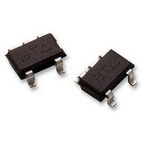
TS9007PCX5 RF Taiwan Semiconductor, TS9007PCX5 RF Datasheet

TS9007PCX5 RF
Specifications of TS9007PCX5 RF
Related parts for TS9007PCX5 RF
TS9007PCX5 RF Summary of contents
Page 1
SOT-25 Pin Definition: 1. Input 2. Ground 3. Enable 4. Bypass 5. Output General Description The TS9007 series is 300mA ultra-low-noise LDO especially designed for battery-power RF and wireless applications. The TS9007 regulator achieves a low 450mV dropout at 300mA ...
Page 2
Absolute Maximum Rating Parameter Supply Voltage Input Supply Voltage (Recommended) Output Short-Circuit Duration Power Dissipation Thermal Resistance Junction Temperature Range Storage Temperature Range Notes: Stress above the listed absolute rating may cause permanent damage to the device. Electrical Characteristics (T ...
Page 3
Application Information Enable / Shutdown The TS9007 comes with and active-high enable pin that allows the regulator to be enabled. Forcing the enable pin low disables the regulator and puts it into the shutdown mode. This pin cannot be left ...
Page 4
Function Description (Continue) Thermal Protection Shutdown The thermal protection shutdown function protects the device from operating in over temperature condition. When the junction temperature exceeds +160 and allowing the IC to tool down. The thermal sensor turns the pass transistor ...
Page 5
Electrical Characteristics Curve Dropout Voltage vs. Load Current Ground Current vs. Input Voltage PSRR vs. Frequency 300mA Low Noise CMOS LDO Dropout Voltage vs. Temperature Output Voltage vs. Temperature PSRR vs. Frequency 5/8 TS9007 Version: A07 ...
Page 6
Marking Diagram 300mA Low Noise CMOS LDO SOT-25 Mechanical Drawing DIM A+ Ө Device Code X = Fixed Output Voltage Code 1=1.2V, A=1.5V, D=1.8V, K=2.5V, M=2.7V, N=2.8V, O=2.9V P=3.0V, S=3.3V ...
Page 7
Marking Diagram DFN 2x2 Mechanical Drawing A = Device Code X = Fixed Output Voltage Code 1=1.2V, A=1.5V, D=1.8V, K=2.5V, M=2.7V, N=2.8V, O=2.9V P=3.0V, S=3. Year Code M = Month Code (A=Jan, B=Feb, C=Mar, D=Apl, E=May, F=Jun, G=Jul, ...
Page 8
Specifications of the products displayed herein are subject to change without notice. TSC or anyone on its behalf, assumes no responsibility or liability for any errors or inaccuracies. Information contained herein is intended to provide a product description only. No ...


